Mar 24 2017
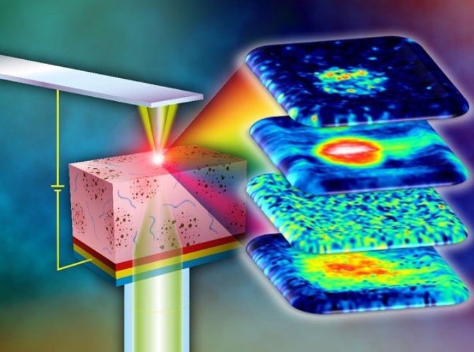
 The STEOM apparatus for multi-parameter characterization of optoelectronic devices at the nanoscale (Credit: National Physical Laboratory (NPL))
A novel measurement technique has been developed by the National Physical Laboratory (NPL) to provide for the first time simultaneous topographical, electrical, chemical and optical microscopy (STEOM) at the nanoscale.
The new technique can be used to enhance the performance of optoelectronic devices such as sensors, organic solar cells, and transistors.
As part of a global collaboration, NPL researchers exhibited the direct application of the new technique to the enhancement of organic solar cells. Transparent, flexible and cost-effective organic solar cells could offer a solution for mass low-carbon energy generation. However, a lack of analytical methods that can concurrently probe device properties at the nanoscale has presented a huge hurdle to their enhancement goal.
The new STEOM technique formulated at NPL addresses this issue, offering concurrent measurements of topography and electrical, chemical and optical properties. The technique is also non-destructive, and does not cause any damage to the samples being measured.
The innovation was accomplished by integrating plasmonic optical signal enhancement with electrical-mode scanning probe microscopy. This allows the relationship between chemical composition, surface morphology, and current generation in operating organic solar cells to be investigated at the nanoscale for the first time.
The researchers showed that information gained using the technique can effectively explain the performance of organic solar cells with regards to the nanoscale composition of their active surface layer, and could be applied to identify the ideal routes for device optimization.
Besides organic solar cells, the technique can be applied to several different issues where nanoscale electronic properties are impacted by surface composition and could as a result be used to guide the design of enhanced optoelectronic devices, from LEDs to sensors.
The research was performed in partnership with Imperial College London, Hangzhou Dianzi University (China), the University of Duisburg-Essen (Germany) and King Abdullah University of Science and Technology (Saudi Arabia). The research paper was published in the Royal Society of Chemistry journal Nanoscale.