Mar 15 2017
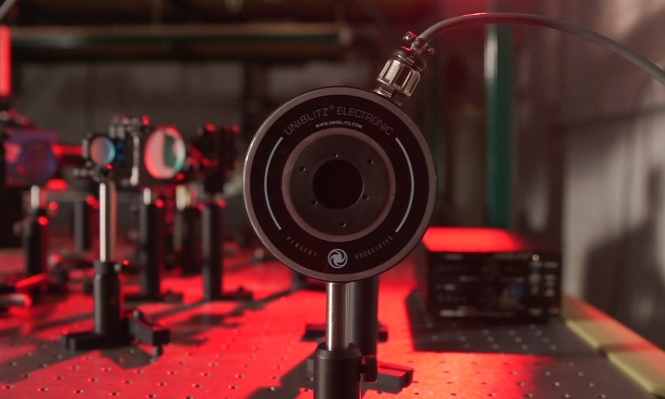
 Researchers at the University�s Institute of Optics developed a technique that uses lasers to render materials hydrophobic�extremely water repellant. CREDIT: University photo/Matthew Mann.
The surface of a material includes minute micro- and nanoscale structures that cannot be seen by the naked eye. However, these structures play a big role in governing the chemical, physical, and biomedical characteristics of the material.
In the recent past, Chunlei Guo and his colleagues from the University of Rochester have discovered many ways to control the structures by irradiating the surface of the material with laser pulses. The researchers changed the materials and made them attract water, repel water, and also absorb huge amounts of light, and they have done all this without the need for any type of coating.
Currently, Guo, Anatoliy Vorobyev, and Ranran Fang, who are researchers from the Institute of Optics at the University of Rochester, have progressed in their research by one more step by creating a method for visualizing, as a first attempt, the complete evolution of formation of the micro- and nanoscale structures on the surface of the material, during and after irradiation with the laser pulse.
After we determined that we could drastically alter the property of a material through creating tiny structures in its surface, the next natural step was to understand how these tiny structures were formed. This is very important because after you understand how they’re formed you can better control them.
Chunlei Guo, University of Rochester
Such manipulation can pave the way for enhancements in all types of technologies such as medical instrumentation, fuel cells, airplane de-icing, energy absorbers, sanitation, space telescopes, and anti-corrosive building materials in third-world countries.
The research team invented a scattered-light imaging method allowing them to record an ultrafast movie of the manner in which the material’s surface is altered by laser radiation. The method has been reported in a paper published in the Nature journal Light: Science & Applications.
The method provides a view of the complete procedure from the time the material is hit by a laser to the melting phase, the transient surface fluctuations, as well as resolidification that results in the formation of permanent micro- and nanostructures.
Currently, it takes about an hour to pattern a metal sample with the dimension of one-inch by one-inch. Determining the manner in which micro- and nanostructures are formed, the researchers can be in a position to streamline the formation of the structures, for example, enhancing the efficiency and speed of patterning surfaces.
The formation and alterations of the small structures render the characteristics to be an intrinsic part of the material, thus minimizing the need for adding temporary chemical coatings.
The research team used a femtosecond laser for producing such effects, where the laser produces an ultra-fast laser pulse of the duration of tens of femtoseconds. One femtosecond is equal to one quadrillionth of a second.
By altering the conditions of the laser, the morphological features of the surface structures, such as their size, geometry, and density, can be changed, thus enabling the material to exhibit a range of distinct physical properties.
Acquiring detailed movies and images of events in micro- and nanoscales is highly difficult as they occur within a few femtoseconds, picoseconds (i.e. one trillionth of a second), or nanoseconds (i.e. one billionth of a second).
For a clearer understanding of the phenomenon, Vorobyev states that light takes approximately one second to travel from Earth to the moon. In contrast, in a nanosecond, light travels just close to one foot, and in a femtosecond, it travels about 0.3 mm, which is nearly equal to the diameter of a bacteria or virus.
A conventional video camera has the ability to record a series of images at the rate of 5 to 30 frames in one second. When the series of images is played in real time, the human eyes observe continuous motion and not a series of separate frames.
Therefore the following question arises: How were Guo and his colleagues successful in recording frames at femtosecond, picosecond, and nanosecond intervals? For achieving this, they employed a method involving scattered light. In a femtosecond laser pulse, the beam is split into two beams: a pump beam targets the material target to bring about alterations in the micro- and nanostructures, and a probe beam functions as a flashbulb, illuminating the process and recording it in a CCD camera, which is a highly-sensitive imaging device that has high resolution.
“We worked very hard to develop this new technique,” stated Guo. “With the scattered light pulsing at femtosecond time intervals, we can capture the very small changes at an extremely fast speed. From these images we can clearly see how the structures start to form.” Guo further added that this scattered light visualization method can be used for capturing any process that occurs on a minute scale. “The technique we developed is not necessarily limited to just studying the surface effects produced in my lab. The foundation we laid in this work is very important for studying ultrafast and tiny changes on a material surface.” This involves the investigation of crystallography, melting, fluid dynamics, and cell activities as well.
The US Army Research Office and the Bill & Melinda Gates Foundation supported this research.
Imaging at the Speed of Light