Apr 27 2010
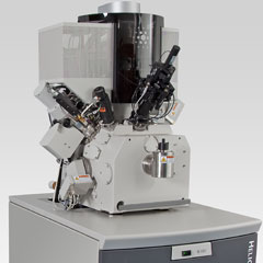
FEI Company (Nasdaq:FEIC), a leading diversified scientific instruments company providing electron and ion-beam microscopes and tools for nanoscale applications across many industries, today introduced the new Helios NanoLab™ x50 DualBeam™ Series, the most powerful and versatile DualBeam system available on the market today. It integrates FEI's extreme high-resolution scanning electron microscope (XHR SEM) with a new, high-performance focused ion beam (FIB), to deliver an unprecedented level of imaging and milling capability for leading-edge applications in semiconductor and materials science research and development.
 Helios NanoLab x50 DualBeam
"FEI was the first to commercialize the DualBeam well over a decade ago, and, in keeping with FEI's long track record of combining the latest in SEM and FIB technologies in a single system, we have unveiled the new Helios NanoLab x50 DualBeam. Designed to meet our customers' next-generation imaging requirements, the Helios is the most capable and flexible dual beam system available on the market today," stated John Williams, FEI's director of corporate and strategic marketing. "It combines unmatched SEM imaging, originally launched in the award-winning Magellan™, and FIB milling performance with improved resolution and stability, for advanced applications in failure analysis, nanoscale characterization, nanoprototyping, sample preparation, and other advanced analytical techniques."
The new high-performance Tomahawk FIB, originally introduced in the V400ACETM and now empowered with FEI's latest fast switching technology, provides unprecedented SEM and FIB live monitoring of milling operations, a smaller FIB spot for more precise milling control, as well as higher beam currents for faster material removal on large structures, such as through silicon vias (TSVs). Overall throughput of advanced TEM lamella preparation has been improved by 40 percent.
"The Helios 450(S) series is designed primarily for today's advanced semiconductor labs that are dealing with numerous challenges, including shrinking dimensions at sub 32nm nodes; advanced packaging techniques, such as TSVs and multi-die stacks; as well as a higher volume of samples requiring TEM imaging," stated Williams.
The Helios 650 is designed for academic and industrial research centers that need to do advanced material characterization and modification down to the single nanometer scale. It delivers a wider range of information and higher quality 3D data in order to better understand material characteristics, such as particle/porosity distribution, crack propagation and other behaviors. The sub-nanometer resolution of the Helios 650 at extremely low beam energies provides surface-specific imaging that, until now, was unavailable in a dual beam instrument. For nanoprototyping, the Helios 650 offers users the ability to create finer, more complex structures over large areas (millimeters in size) with better control over dimensions, fewer artifacts, faster material removal rates, and more.