Dec 17 2009
Techniques recently invented by researchers at the California Institute of Technology (Caltech)—which allow the real-time, real-space visualization of fleeting changes in the structure of nanoscale matter—have been used to image the evanescent electrical fields produced by the interaction of electrons and photons, and to track changes in atomic-scale structures.
Papers describing the novel technologies appear in the December 17 issue of Nature and the October 30 issue of Science.
Four-dimensional (4D) microscopy—the methodology upon which the new techniques were based—was developed at Caltech's Physical Biology Center for Ultrafast Science and Technology. The center is directed by Ahmed Zewail, the Linus Pauling Professor of Chemistry and professor of physics at Caltech, and winner of the 1999 Nobel Prize in Chemistry.
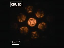
 This is the diffraction obtained for silicon with 4D electron microscopy. The nanoscale can be determined from the patterns the structure.
Zewail was awarded the Nobel Prize for pioneering the science of femtochemistry, the use of ultrashort laser flashes to observe fundamental chemical reactions occurring at the timescale of the femtosecond (one-millionth of a billionth of a second). The work "captured atoms and molecules in motion," Zewail says, but while snapshots of such molecules provide the "time dimension" of chemical reactions, they don't give the dimensions of space of those reactions—that is, their structure or architecture.
Zewail and his colleagues were able to visualize the missing architecture through 4D microscopy, which employs single electrons to introduce the dimension of time into traditional high-resolution electron microscopy, thus providing a way to see the changing structure of complex systems at the atomic scale.
In the research detailed in the Science paper, Zewail and postdoctoral scholar Aycan Yurtsever were able to focus an electron beam onto a specific nanoscale-sized site in a specimen, making it possible to observe structures within that localized area at the atomic level.
In electron diffraction, an object is illuminated with a beam of electrons. The electrons bounce off the atoms in the object, then scatter and strike a detector. The patterns produced on the detector provide information about the arrangement of the atoms in the material. However, if the atoms are in motion, the patterns will be blurred, obscuring details about small-scale variations in the material.
The new technique devised by Zewail and Yurtsever addresses the blurring problem by using electron pulses instead of a steady electron beam. The sample under study—in the case of the Science paper, a wafer of crystalline silicon—is first heated by being struck with a short pulse of laser light. The sample is then hit with a femtosecond pulse of electrons, which bounce off the atoms, producing a diffraction pattern on a detector.
Since the electron pulses are so incredibly brief, the heated atoms don't have time to move much; this shorter "exposure time" produces a sharp image. By adjusting the delay between when the sample is heated and when the image is taken, the scientists can build up a library of still images that can be strung together into a movie.
"Essentially all of the specimens we deal with are heterogeneous," Zewail explains, with varying compositions over very small areas. "This technique provides the means for examining local sites in materials and biological structures, with a spatial resolution of a nanometer or less, and time resolution of femtoseconds."
The new diffraction method allows the structures of materials to be mapped out at an atomic scale. With the second technique—introduced in the Nature paper, which was coauthored by postdoctoral scholars Brett Barwick and David Flannigan—the light produced by such nanostructures can be imaged and mapped.
The concept behind this technique involves the interaction between electrons and photons. Photons generate an evanescent field in nanostructures, and electrons can gain energy from such fields, which makes them visible in the 4D microscope.
In what is known as the photon-induced near-field electron microscopy (PINEM) effect, certain materials—after being hit with laser pulses—continue to "glow" for a short but measurable amount of time (on the order of tens to hundreds of femtoseconds).
In their experiment, the researchers illuminated carbon nanotubes and silver nanowires with short pulses of laser light as electrons were being shot past. The evanescent field persisted for femtoseconds, and the electrons picked up energy during this time in discrete amounts (or quanta) corresponding to the wavelength of the laser light. The energy of an electron at 200 kilo-electron volts (keV) increased by 2.4 electron volts (eV), or by 4.8 eV, or by 7.2 eV, etc.; alternatively, an electron might not change in energy at all. The number of electrons showing a change is more striking if the timing is just right, i.e., if the electrons are passing the material when the field is at its strongest.
The power of this technique is that it provides a way to visualize the evanescent field when the electrons that have gained energy are selectively identified, and to image the nanostructures themselves when electrons that have not gained energy are selected.
"As noted by the reviewers of this paper, this technique of visualization opens new vistas of imaging with the potential to impact fields such as plasmonics, photonics, and related disciplines," Zewail says. "What is interesting from a fundamental physics point of view is that we are able to image photons using electrons. Traditionally, because of the mismatch between the energy and momentum of electrons and photons, we did not expect the strength of the PINEM effect, or the ability to visualize it in space and time."