Reviewed by Lexie CornerFeb 27 2024
With the help of “accelerator-on-a-chip” technology, Stanford researchers are getting closer to creating a tiny electron accelerator that could have various applications in industry, medicine, and physics research.
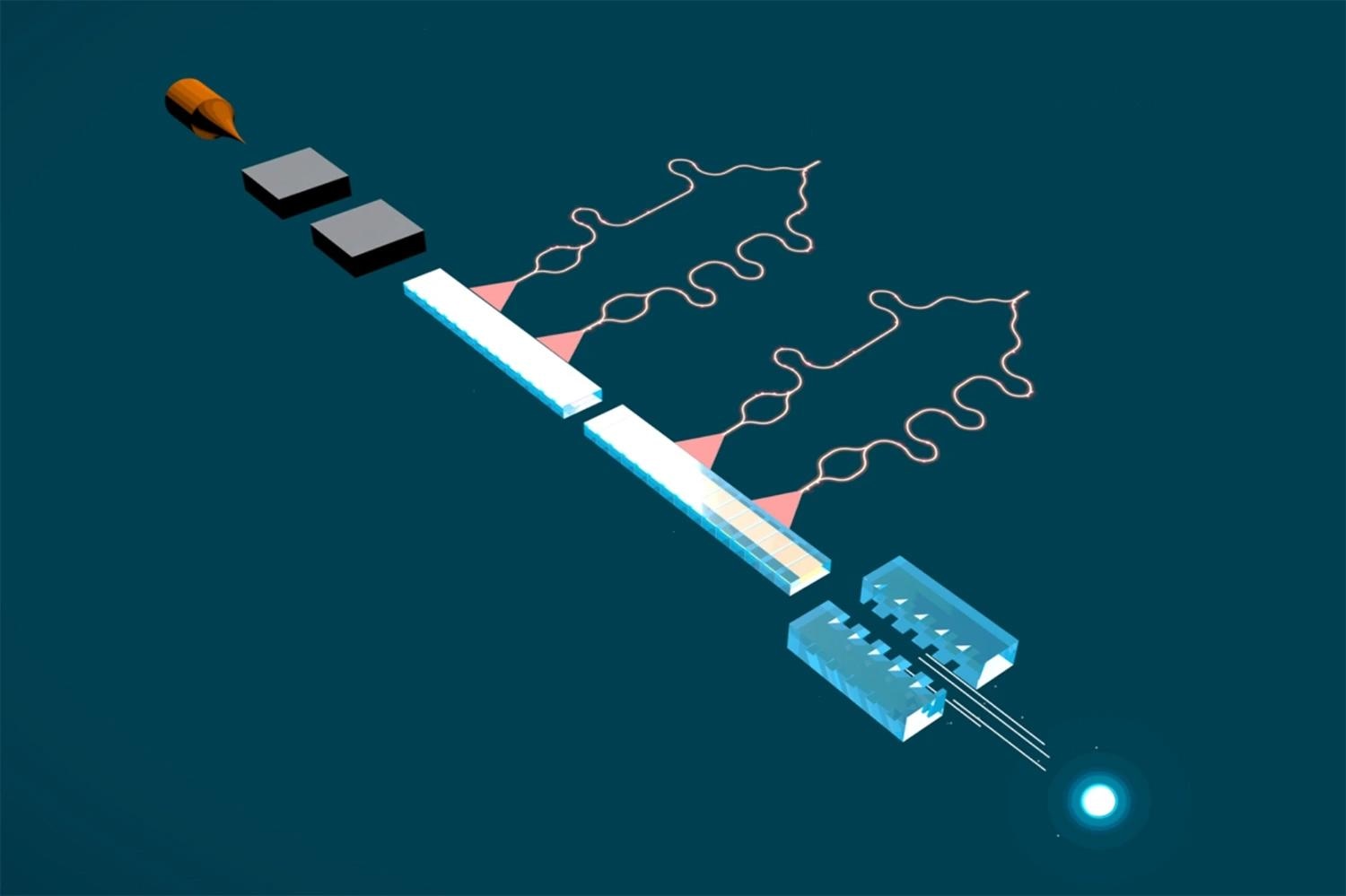
 Illustration of a shoebox-sized accelerator. An electron source and buncher/injector feed into a sub-relativistic DLA (the device described in this article), which accelerates electrons up to 1 MeV in energy. These electrons are further accelerated by SiO2 waveguide-driven relativistic DLA and finally pass through an undulator to produce coherent free-electron radiation. Image Credit: Moore Foundation/Payton Broaddus.
Scientists have shown that electrons can now be accelerated and confined using a silicon dielectric laser accelerator, or DLA, producing a concentrated beam of high-energy electrons. The study was published in the journal Physical Review Letters.
If the electrons were microscopic cars, it's as if, for the first time, we're steering, and we have our foot on the gas.
Payton Broaddus, Ph.D., Department of Electrical Engineering, Stanford University
Taking Accelerators From Miles to Microns
High-energy particle beams produced by accelerators enable physicists to investigate material properties, create targeted probes for medical applications, and pinpoint the fundamental components of matter that comprise the universe. Developed in the 1930s, some of the earliest high-energy particle accelerators were small enough to fit on a tabletop.
However, higher particle energies were needed to study more complex physics, which meant that scientists had to construct larger systems. The original linear accelerator tunnel at SLAC National Accelerator Laboratory on the Stanford campus was put into service in 1966—it is nearly 2 miles long.
There’s the ability to just completely replace every other particle accelerator with something that’s cheaper and smaller.
Payton Broaddus, Ph.D., Department of Electrical Engineering, Stanford University
Olav Solgaard, the senior author of the paper and Director of the Edward L. Ginzton Laboratory as well as the Robert L. and Audrey S. Hancock Professor in the School of Engineering, stated that this vision is becoming more and more feasible due to advancements in nano-scale fabrication and lasers. Conventional radiofrequency accelerators consist of radio waves pumped into copper cavities, increasing the energy of the particles.
As the metal may get heated by these pulses, the cavities must function at lower energy and pulse rates to dissipate the heat and prevent melting.
However, glass and silicon structures can be much more powerful and smaller because they can withstand higher-energy laser pulses without overheating. Researchers at Stanford University began experimenting with these materials’ nanoscale structures approximately ten years ago. In 2013, a group led by Robert Byer, William R. Kenan Jr. Professor Emeritus and co-author of the paper, demonstrated that electrons could be successfully accelerated by a tiny glass accelerator that pulsed infrared light.
Due to these outcomes, the Gordon and Betty Moore Foundation accepted the project as part of the global Accelerator on a Chip (ACHIP) collaboration, aiming to create a mega-electron-volt accelerator the size of a shoebox.
However, issues with the initial “accelerator on a chip” remained. According to Broaddus, the electrons inside were like cars on a narrow road without steering wheels—they could hit a wall with equal ease and tremendous acceleration.
Steering Electrons With Lasers
The Stanford research team has now successfully demonstrated their ability to control electrons at the nanoscale. To achieve this, they created a silicon structure with a sub-micron channel in a vacuum system. They put electrons into one end and used a shaped laser pulse that produced kinetic energy kicks to illuminate the structure from both sides. The electrons were kept from veering off course by the periodic flipping between the focusing and defocusing properties of the laser fields.
The electrons were impacted by this sequence of acceleration, defocusing, and focusing over a nearly millimeter. Though it may not seem like much, these charged particles experienced a significant boost in energy, increasing by 23.7 kilo-electron volts, or about 25 %, over their initial energy. The team’s prototype tiny accelerator has accelerated at a rate comparable to traditional copper accelerators, and Broaddus says much higher acceleration rates are achievable.
Even though it is a big step in the right direction, more work must be done before these tiny accelerators are applied in business, healthcare, and research. The team has only been able to steer electrons in two dimensions; three-dimensional electron confinement will be needed to extend the accelerator long enough to achieve higher energy gains.
Electron Relay Race
Broaddus mentioned that a sister research group at Friedrich Alexander University (FAU) in Erlangen, Germany, recently showcased a comparable device utilizing a single laser and commencing at significantly lower initial energy levels. He indicated that both the FAU device and the Stanford device would eventually form part of what he described as an electron relay race.
Three people will participate in this upcoming relay. After receiving an initial boost from the FAU device, low-energy electrons could be fed into a device resembling the one Broaddus is creating. For the electrons, the final step would be an accelerator composed of glass, similar to the one Byer created. As glass is more resistant to laser radiation than silicon, the accelerator can energize the electrons even more and accelerate them toward the speed of light.
Solgaard thinks that eventually, just like its larger counterparts, such a tiny accelerator will be helpful in high-energy physics, probing the basic matter that constitutes the universe. While "we have a very, very long way to go," Solgaard remains optimistic, adding that "we've taken the first few steps."
Journal Reference:
Broaddus, P., et al. (2024) Subrelativistic Alternating Phase Focusing Dielectric Laser Accelerators. Physical Review Letters. doi.org/10.1103/PhysRevLett.132.085001