Based on earlier outstanding reviews in the area of defect inspection methods, defect inspection researchers from Huazhong University of Science and Technology, Harbin Institute of Technology, and The Chinese University of Hong Kong conducted a thorough analysis of fresh perspectives and thrilling trends.
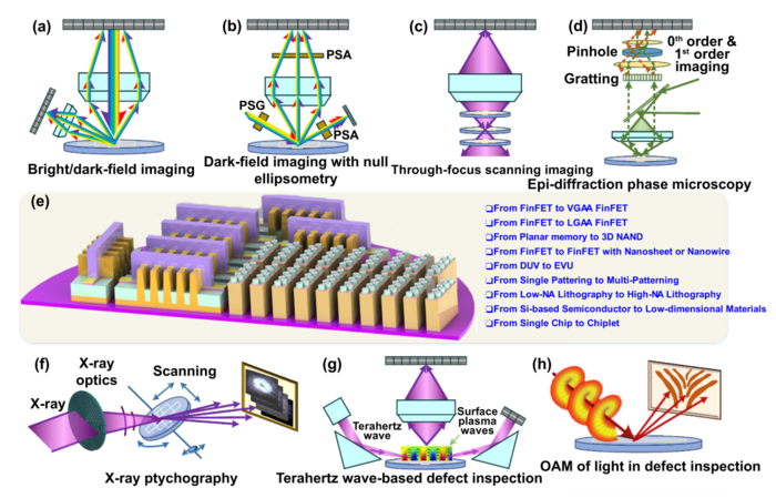
 Diverse optical wafer defect inspection systems including (a) Brightfield/darkfield imaging system, (b) Dark-field imaging with null ellipsometry, (c) Through-focus scanning imaging microscopy, (d) Epi-diffraction phase microscopy, (e) Patterned wafer containing logic dies, and 3D NAND memory dies, (f) X-ray ptychography, (g) THz wave-based defect inspection system, and (h) Coherent Fourier scatterometry techniques using different OAM illumination beams. Image Credit: Jinlong Zhu, Jiamin Liu, Tia
This review covers the evaluation of defect detectability, the various optical inspection methods, and the post-processing algorithms.
The Nanoscale and Optical Metrology Research Center (NOMRC), under the direction of Professor Shiyuan Liu and Professor Jinlong Zhu from Huazhong University of Science and Technology and their partners from the Harbin Institute of Technology and The Chinese University of Hong Kong, published the first literature review to communicate the most recent advancements and the trend of optical wafer defect inspection.
The International Journal of Extreme Manufacturing published this study, showing that state-of-the-art methods can significantly influence sub-10 nm defect inspection, including nanophotonics, optical vortices, computational images, quantitative phase imaging, and deep learning. The research could open up new possibilities for semiconductor wafer flaw inspection.
Professors Zhu and Liu stated, “The ever-shrinking features and space on patterned wafers would dramatically strain the capabilities of all the current metrology and inspection solutions in balancing sensitivity, specificity, process speed, and capture rate.”
Optical far-field wafer inspection is one of the mainstays for defect inspection in the fab. A traditional defect inspection tool compares the circuit pattern images of nearby dies to identify the faults.
The key to defect inspection is not resolution, but the signal-to-noise ratio (SNR) and contrast.
Jinlong Zhu, Study First Author and Professor, Nanoscale and Optical Metrology Research Center
“The improvement of SNR and contrast highly depends on sophisticated instruments, advanced modeling architectures and post-processing algorithms, all of which drove us to make a comprehensive review of wafer defect detection methods from the following three aspects: 1) the defect detectability evaluation, (2) the diverse optical inspection systems, and (3) the post-processing algorithms,” Zhu added.
It is of great importance to carry out defect detectability assessment for a specific type of inspection tools for advanced nodes.
Dr Jiamin Liu, Study Co-First Author and Professor, Nanoscale and Optical Metrology Research Center
“The evaluation of defect detectability usually involves the formulation of quantitative rules for the SNR of the defect scattering signals, the development of simulation tools for defect scattering signals modeling, and the analysis of defect SNR. We found the defect SNR depends significantly on material and defect topology,” he said.
How to use the traditional methods of optical defect inspection, like the amplitude-based method and its post-processing algorithms, has been extensively explored.
The possibilities of the innovative inspection processes, which include ones based on phase, orbital angular momentum, terahertz waves, and hyperbolic Bloch modes, have been highlighted to draw the readers' attention.
The article also evaluated and prospected in-depth X-ray ptychography, the only optical technique that can directly image surface and undersurface sub-20 nm flaws for the entire wafer. In the future, once the limitations associated with the synchrotron X-ray light source, a vast amount of data, and the slow pace are overcome, X-ray ptychography has the potential to infiltrate the field by offering revolutionary 3D resolution and sensitivity.
“Whether it is the simplest image difference operator or the complex image synthetic algorithm or even the deep learning algorithms, these post-processing algorithms play a critical role in optical defect inspection in terms of improving SNR and contrast of defects,” co-first author Dr Tianlai Xu further added.
“Therefore, we provided a detailed discussion of post-processing algorithms involved in patterned wafer defect inspection with a specific focus on the advantages and disadvantages of deep learning algorithms,” he said.
Prof. Jinlong Zhu said, “We do believe that optical defect inspection on patterned wafers will remain a challenging but interesting topic that urgently needs to be addressed. We believe this review article, which is written based on reviews and some exploratory research in the cutting-edge direction is important to both new entrants in the field and those who are seeking to use it in interdisciplinary work.”
Journal Reference:
Zhu, J., et al. (2022) Optical wafer defect inspection at the 10 nm technology node and beyond. International Journal of Extreme Manufacturing. doi.org/10.1088/2631-7990/ac64d7.