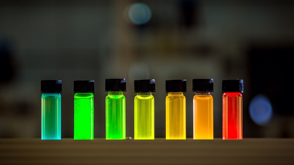
In a pre-proof study from Organic Electronics, researchers have used the photolithographic method to design high-resolution, highly efficient quantum dot light-emitting diodes (QLEDs) patterned by ultraviolet-induced ligand exchange. This paves the way for the development of next-generation high-resolution displays.

Study: High-Performance, High-Resolution Quantum Dot Light-Emitting Devices Through Photolithographic Patterning. Image Credit: Tayfun Ruzgar/Shutterstock.com
Displays play a crucial part in the modern information society, which creates an endless demand for new and improved products and technology. High-resolution displays are becoming the focus of new technology requirements. Quantum dot light-emitting diodes are one of the more intriguing upcoming technologies due to their potential to attain high resolution using photolithography.
Significance of Quantum Dot Light-Emitting Diodes in High-Resolution Displays
Different display techniques have been created over the past few decades to enhance quality and fulfill the expanding needs of information distribution.
High resolution will be necessary for the next-generation displays in the near future due to the demand for near-eye display technology and the production of enormous information.
However, as pixel size continues to shrink, the current dominant research hotspots, such as micro-light-emitting diodes and organic light-emitting diodes, are forced to deal with inescapable problems such as high driving voltage, sidewall edge effect, and low luminance, resulting in substantial performance degradation.
Quantum dot light-emitting diodes are an attractive option for the next generation of high-quality displays due to their high luminescence efficiency, narrow emission bandwidth, rich color gamut, customizable emission wavelength, and excellent photostability.
Moreover, quantum dot light-emitting diodes are based on nano-sized quantum dots (QDs), whose performance is theoretically unaffected by pixel size and is therefore appropriate for producing high-resolution displays.
Techniques to Design QLED Pixel and Their Limitations
Quantum dot light-emitting diode pixel patterns are generated using inkjet printing (IJP), photolithography, and transfer printing.
Inkjet printing
The IJP technique encounters difficulties in producing microscopic pixels smaller than tens of microns. Controlling nanoparticles in a specific area of the printed ink and the influence of a three-phase contact line results in uneven quantum dot films and poor device performance.
Transfer printing
Transfer printing's unique ability to prepare ultra-small pixels is hampered by elastic stamp peeling and sagging, which adversely influence film morphology and quality. It is challenging to fabricate high-resolution, all-color gadgets in this process because it is difficult to position the stamp precisely at ultra-small scales.
Photolithography
Photolithography is a proven technology frequently employed in display devices and can create high-precision sub-pixels via a photochemical reaction. This technique is popular for patterning quantum dot films.
However, photolithography alters the properties of quantum dot ligands and can generate new surface flaws, resulting in a noticeable reduction in device performance.
Using an Improved Photolithography Based On Ultraviolet-Induced Ligand Exchange
A high-resolution photolithographic patterning with no photoresist was performed. The quantum dot's surface ligands are exchanged under ultraviolet irradiation by including a photo-acid generator in the quantum dot films, resulting in a QD solubility switch.
An in situ ligand exchange technique helped vary the QDs' dissolution rate in the mother liquor to pattern the quantum dot films.
A concentration of 1.2 mg/ml of 2-(4Methoxystyryl)-4,6 bis(trichloromethyl)-1,3,5-triazine (MBT) created green, red, and blue quantum dot arrays with varying pattern sizes.
After the ligand exchange, afresh passivation was conducted to clean the patterned quantum dot's surface flaws.
A polymethyl methacrylate film was placed as a charge barrier layer to prevent direct contact between the electron and hole transport layers.
Important Findings of the Study
Compared with the unmodified (non-patterned) QLED device, the performance of the quantum dot light-emitting diode following ligand exchange is decreased. This can be due to the surface damage or unsaturated ligand passivation of the quantum dots induced by the free radicals produced during the chemical reaction process.
Photoluminescence and electroluminescence in quantum dots are enhanced by 1,2-ethanedithiol (EDT) passivation, leading to a three-fold increase in system efficiency.
The leakage current in the non-luminance area between QD arrays is minimized when a polymethyl methacrylate film is applied as a charge barrier layer to isolate the electron and hole transport layers from direct contact.
High-performance quantum dot light-emitting diodes with a 5 μm pixel diameter were developed by enhancing ligand passivation and effectively lowering leakage current. The quantum dot light-emitting diodes had a luminance of 125,000 cd/m2.
By altering the thickness of the polymethyl methacrylate barrier layer, the quantum dot light-emitting diodes demonstrated low-efficiency roll-off, and maximum external quantum efficiency of 10.5% was achieved.
This research lays the groundwork for achieving high-performance, high-resolution QLEDs for next-generation display applications.
Reference
H. Gao, Y. Qie, H. Zhao, F. Li, T. Guo, H. Hu. (2022). High-Performance, High-Resolution Quantum Dot Light-Emitting Devices Through Photolithographic Patterning. Organic Electronics. https://www.sciencedirect.com/science/article/abs/pii/S1566119922001811
Disclaimer: The views expressed here are those of the author expressed in their private capacity and do not necessarily represent the views of AZoM.com Limited T/A AZoNetwork the owner and operator of this website. This disclaimer forms part of the Terms and conditions of use of this website.