The world is experienced by humans in three dimensions. However, a research partnership in Japan has formulated a method to develop synthetic dimensions to better comprehend the fundamental laws of the universe and perhaps apply them to modern technologies.
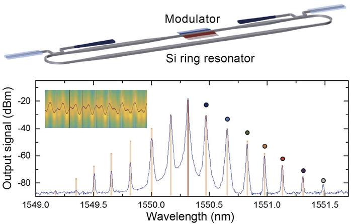
 Ring resonator fabricated using silicon photonics and modulated internally generates a frequency ladder. (Image Credit: Yokohama National University).
The results of the study have been published in the January 28, 2022 issue of Science Advances.
The concept of dimensionality has become a central fixture in diverse fields of contemporary physics and technology in past years. While inquiries into lower-dimensional materials and structures have been fruitful, rapid advances in topology have uncovered a further abundance of potentially useful phenomena depending on the dimensionality of the system, even going beyond the three spatial dimensions available in the world around us.
Toshihiko Baba, Study Author and Professor, Department of Electrical and Computer Engineering, Yokohama National University
Topology denotes an extension of geometry that mathematically illustrates spaces with properties maintained in continuous distortion, for example, the twist of a Möbius strip. When integrated with light, according to Baba, these physical spaces can be guided in a way that allows scientists to trigger extremely complicated phenomena.
In everyday life, from a line to a cube to a square, each dimension offers more information and requires more knowledge to precisely define it. In topological photonics, scientists can develop extra dimensions of a system, permitting more degrees of freedom and complex manipulation of properties formerly not possible.
“Synthetic dimensions have made it possible to exploit higher-dimensional concepts in lower-dimensional devices with reduced complexity, as well as driving critical device functionalities such as on-chip optical isolation,” Baba said.
The scientists created a synthetic dimension on a silicon ring resonator, with the help of the same approach used to construct complementary metal-oxide-semiconductors (CMOS), a computer chip that can store a little amount of memory. A ring resonator applies guides to regulate and divide light waves according to definite parameters, such as specific bandwidths.
According to Baba, the silicon ring resonator photonic device obtained “comb-like” optical spectra, creating coupled modes equivalent to a one-dimensional model. Simply put, the device created a measurable property — a synthetic dimension — that enabled the scientists to deduce information relating to the rest of the system.
While the newly formed device includes one ring, more could be stacked to cascade effects and rapidly characterize optical frequency signals.
Critically, Baba said, their system, even with stacked rings, is a lot smaller and compact than earlier approaches, which used optical fibers linked to different components.
A more scalable silicon photonic chip platform provides a considerable advancement, as it allows photonics with synthetic dimensions to benefit from the mature and sophisticated CMOS commercial fabrication toolbox, while also creating the means for multi-dimensional topological phenomena to be introduced into novel device applications.
Toshihiko Baba, Study Author and Professor, Department of Electrical and Computer Engineering, Yokohama National University
The system’s flexibility, including the capability to reconfigure it as required, complements corresponding static spaces in real space, which could help scientists avoid the dimensional limitations of real space to comprehend phenomena outside of the three dimensions, according to Baba.
This work shows the possibility that topological and synthetic dimension photonics can be used practically with a silicon photonics integration platform. Next, we plan to collect all topological and synthetic dimension photonic elements to build up a topological integrated circuit.
Toshihiko Baba, Study Author and Professor, Department of Electrical and Computer Engineering, Yokohama National University
Other contributors include Armandas Balčytis and Jun Maeda, Department of Electrical and Computer Engineering, Yokohama National University; Tomoki Ozawa, Advanced Institute for Materials Research, Tohoku University; and Yasutomo Ota and Satoshi Iwamoto, Institute for Nano Quantum Information Electronics, The University of Tokyo.
Ota is also affiliated with the Department of Applied Physics and Physico-Informatics, Keio University. Iwamoto is also affiliated with the Research Center for Advanced Science and Technology and the Institute of Industrial Science, The University of Tokyo.
This research was supported by the Japan Science and Technology Agency (JPMJCR19T1, JPMJPR19L2), the Japan Society for the Promotion of Science (JP20H01845) and RIKEN.
Journal Reference:
Balčytis, A., et al. (2022) Synthetic dimension band structures on a Si CMOS photonic platform. Science Advances. doi.org/10.1126/sciadv.abk0468.