Apr 23 2020
According to scientists, optical fiber communications may soon become more energy efficient, thanks to a recent discovery made by a U.S. Army study on optoelectronic devices.
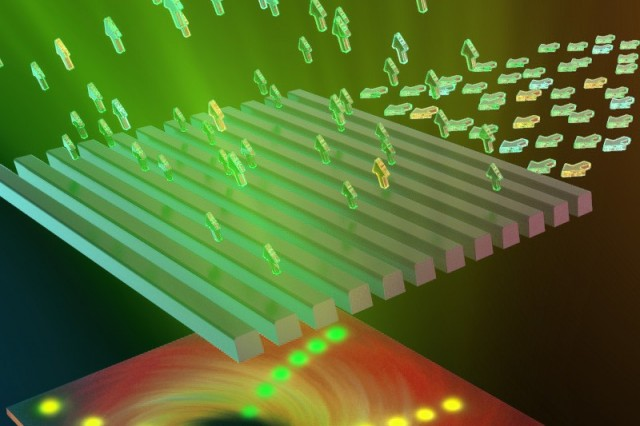
 Army-funded researchers developed a new design of optical devices that could help make optical fiber communications more energy efficient. Image Credit: University of Pennsylvania.
The University of Pennsylvania, Massachusetts Institute of Technology, and Peking University have teamed up to work on a new project that was partly funded by the Army Research Office—a part of the U.S. Army Combat Capabilities Development Command’s Army Research Laboratory.
The aim of the project was to create an innovatively designed optical device that emits light only in one direction. This one-sided radiation channel meant for light can be employed in many different optoelectronic applications to minimize the energy loss that occurs in data centers and optical fiber networks. The findings were published in the Nature journal.
Light can travel in optical fibers along a single direction, similar to how water moves through a pipe. Fibers are connected to chip by using on-chip couplers. Light signals within the chips are produced, amplified, or identified. While most of the light traveling via the coupler continues to move through to the fiber, some part of the light moves in the reverse direction and thus escapes.
This radiation loss accounts for a major part of energy usage in data traffic. In fact, the total consumption of energy in data centers is 2% of the worldwide electricity demand, with demands rising each year.
It was consistently proposed by earlier studies that a minimal energy loss of about 25% at each interface between the chips and optical fibers was a theoretical upper limit, which could not be exceeded. Since interwoven and complex systems of nodes are needed by data centers, that 25% of energy loss rapidly increases as light moves via a network.
You may need to pass five nodes (10 interfaces) to communicate with another server in a typical medium-sized data center, leading to a total loss of 95 percent if you use existing devices. In fact, extra energy and elements are needed to amplify and relay the signal again and again, which introduces noise, lowers signal-to-noise ratio, and, ultimately, reduces communication bandwidth.
Jicheng Jin, Doctoral Student, University of Pennsylvania
When the researchers thoroughly analyzed the system, they found that the energy loss could be reduced nearly to zero by breaking the left-right symmetry in their new device.
These exciting results have the potential to spur new research investments for Army systems. Not only do the coupling efficiency advances have potential to improve data communications for commercial data centers, but the results carry huge impact for photonic systems where much lower intensity signals can be used for the same precision computation, making battery powered photonic computers possible.
Dr Michael Gerhold, Program Manager, Optoelectronics, Army Research Office
To gain a deeper understanding of this phenomenon, the researchers proposed a theory on the basis of topological charges. These topological charges prevent radiation in a certain direction. For a coupler featuring both the left-right and up-down symmetries, a single charge is available on each side, preventing the radiation from traveling in the vertical direction.
Imagine it as two-part glue. By breaking the left-right symmetry, the topological charge is split into two half charges—the two-part glue is separated so each part can flow. By breaking the up-down symmetry, each part flows differently on the top and the bottom, so the two-part glue combines only on the bottom, eliminating radiation in that direction. It’s like a leaky pipe has been fixed with a topological two-part glue.
Bo Zhen, Assistant Professor, Department of Physics and Astronomy, University of Pennsylvania
In the end, the researchers settled on a design that has a range of slanted bars, which break both the up-down and left-right symmetries, simultaneously. To develop these structures, the team created a new etching technique. This method involves placing silicon chips on a wedge-like substrate and enabling the etching process to take place at a slanted angle.
By contrast, typical etchers are only capable of producing vertical sidewalls. As a next step, the researchers are hoping to further improve this etching method so that it can be used with contemporary foundry processes. The team is also planning to develop a relatively simpler design for etching purposes.
The authors of the study are anticipating to apply this method in technologies where light can move more efficiently at short distances, such as between a chip in a server and an optical fiber cable, and even across longer distances, like long-range Lidar systems.
The Air Force Research Laboratory, Natural Science Foundation of China, MIT Lincoln Laboratory, and HPCP of Peking University also financially supported this study.