Aug 24 2018
One-dimensional (1D) nanostructures have a smaller size, larger surface-to-volume ratio, and higher carrier mobility when compared to conventional thin-film photodetectors.
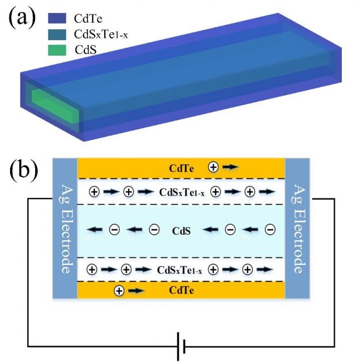
 (a) The schematic diagram of CdS-CdSxTe1-x-CdTe nanobelts. (b) Schematic diagram of electron-hole pair separation and transfer in the CdS-CdSxTe1-x-CdTe heterostructure photodetector. (Image Credit: ©Science China Press)
As a result, these nanostructures are likely to have larger internal gain and higher sensitivity, which make them potential candidates in everyday applications, for example, imaging, optical communication, and single photon detecting.
CdS is a representative II-VI semiconductor and hence it is a potential material in the detection of visible-UV light. However, in the case of pure NWs/NBs-based photodetectors, it is not possible to achieve high sensitivity and rapid photoresponse speed at the same time due to the surface reaction.
In recent times, a group of Qing Yang in Zhejiang University showed a CdS-CdSxTe1-x-CdTe core-shell nanobelt photodetector, which has both fast speed and high sensitivity. To fabricate the CdS-CdSxTe1-x-CdTe nanobelts, CdTe was introduced in the growth of CdS nanobelt. Due to the unique growth condition, layers of ternary crystal CdSxTe1-x alloy were formed between CdTe and CdS and layers, which eventually resulted in the formation of the CdS-CdSxTe1-x-CdTe core-shell structure.
This photodetector was shown to have the fastest response time of 11µs, which is the fastest CdS-based nanobelt photodetector. The improved response speed is attributed to the formation of heterojunction among CdTe, CdSxTe1-x, and CdS layers, which tend to suppress the surface reaction. The detection light spectrum has also covered a broad range between 355 and 785 nm.
When compared to pure CdTe or CdS nanostructure-based photodetectors, the detection spectrum of the nanobelt photodetector is found to be much extended, encompassing the entire visible spectrum. The 3 dB bandwidth and responsivity of the nanobelt photodetector reach up to 22.9 KHz and 1520 A/W, respectively. Since the CdS-CdSxTe1-x-CdTe NB involve a simple fabrication process, have good response speed, excellent performance in responsivity, and detection spectrum, they can potentially be used in many optoelectronic nano devices, for example, imaging, sensing, and optical communications.