Jul 4 2017
The world’s most narrowband diode laser on a chip has been developed by Researchers from the University of Twente’s MESA+ research institute in collaboration with the Lionix company.
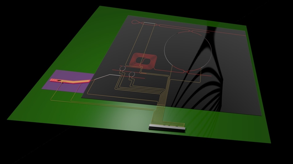
 hybrid laser 3d-view Credit: University of Twente
This laser represents advancement in the rapidly growing field of photonics, and will help in bringing applications like accurate GPS and 5G internet closer. Professor Klaus Boller, Research Leader, presented the research findings during an esteemed scientific conference in Munich.
Individuals are gradually reaching the bounds of what is possible with electronics. This is the reason why the private sector and Scientists are dedicated to photonics – a significant technology that makes several other innovations possible. This includes the use of light particles (photons) for transporting and processing data.
It is essential to correctly control the light signals in order to allow photonic chips to function as efficiently as possible. This explains the fact that all the light particles that are transmitted must have, as closely as possible, the very same frequency, this is, the same color. Researchers from the University of Twente have succeeded in developing a tiny laser on a chip with a maximum bandwidth (the maximum uncertainty of frequency) of only 290 Hertz. By some distance, this is considered to be the most precise laser on a chip that has ever been developed.
Our signal is more than ten times more coherent – or clean – than any other laser on a chip.
Professor Klaus Boller, Research Leader
The new laser is tunable, meaning that users can select the color of the laser by themselves, from a wide range of colors. The device is considered to be a hybrid laser since it comprises of two varied photonic chips, optically connected to each other.
Photonics in Twente
The record laser will introduce innumerable applications within reach. Some of these applications include controlling movable antennae on phone masts for 5G mobile internet, more rapid data flows via glass fiber networks, or more accurate sensors and GPS systems for monitoring the structural integrity of bridges and buildings.
Twente is a leading region in the world when talking about photonics, which is blooming into an industry worth billions given that the technology is considered key to a huge number of applications. The region is, for instance, the birthplace of the TriPleX technology, one of the extremely vital standards for photonic chips. The deep expertise and the strong chemistry between all stakeholders are present at the heart of Twente’s strong position. The complete innovation chain is here and cooperation is indeed intense: from basic science in a wide range of key domains to firms that stand among the world’s best when it comes to production, development and the incorporation of components.
Research
The research was executed by Youwen Fan and Klaus Boller of the Laser Physics and Nonlinear Optics department at the University of Twente MESA+ research institute, Applied Nanophotonics, in partnership with Ruud Oldenbeuving, Chris Roeloffzen, Marcel Hoekman, Dimitri Geskus, and René Heideman of the company LioniXInternational.