Apr 6 2017
In high precision industries, the optical microscope is an important piece of equipment for failure inspection and scientific research. However, for hundreds of years the imaging resolution of microscopes is fundamentally constrained by the diffraction limit of light. Current efforts to circumvent this fundamental diffraction limit by using various technologies have not succeeded because of factors such as a near-field operation, requiring the sample to be proximal to the microscope, or the dyeing of samples, an invasive process affecting the quality of the sample.
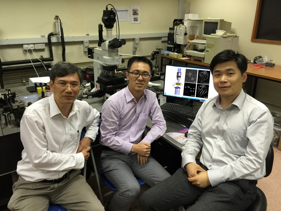
 A team of researchers from the National University of Singapore's Faculty of Engineering has developed a novel lens for super-resolution imaging which breaks resolution limitations in microscopy and has potential applications in high precision failure inspection and biological research. (L-R) Professor Hong Minghui, Dr Qin Fei and Associate Professor Qiu Cheng Wei. Credit: National University of Singapore
Now a new supercritical lens has been developed by a research group led by Professor Hong Minghui and Associate Professor Qiu Cheng Wei from the Department of Electrical and Computer Engineering at the National University of Singapore (NUS) Faculty of Engineering. This lens enables optical microscopes to shoot pictures in real-time with more detail, beyond diffraction limit. Moreover, the strategy requires no post-processing of the image or pre-treatment of samples.
Our breakthrough is achieved in a totally non-invasive manner, coupled with the capability of real-time imaging. This could potentially open up a wide range of applications in areas such as high precision failure inspection in the semiconductor industry, and will also contribute significantly to biological research.
Prof Hong
High-performance, ultra-thin lens that is easy to fabricate at low cost
In contrast to the conventional three-dimensional bulky optical lens, the planar metalens is an ultra-thin, high-performance lens with extraordinary capabilities in light modulation. The supercritical lens, developed by the NUS team, is based on the concept of an optimized planar metalens. The supercritical lens has been developed by employing a new algorithm, and can be conveniently fabricated using a commercial laser pattern generator at low cost and in high speed.
The NUS team used a supercritical lens microscope to show an imaging resolution of 65 nm, as compared to resolutions of around 120 to 150 nm that are obtained by using typical microscopes. Additionally, the new microscopy method exhibits a considerably longer working distance of 55 μm, which ensures additional working space for convenient handling and adjustment of samples in real-world applications, and allowing a more detailed observation of the samples.
Using a lens with microscale feature size, we have achieved nanoscale imaging resolution. Our invention could potentially bridge the wide gap between laboratory proof-of-concept demonstrations and practical applications for the super-resolution imaging technique.
Assoc Prof Qiu
Wide-ranging applications
NUS researchers’ discovery has a lot of potential for nano-imaging of semiconductor devices. It can potentially enable detection of defects in components such as integrated circuit chips in a cost-effective, quicker, and in a more accurate manner.Such detection techniques necessitate imaging resolution of less than 100 nm (sub-diffraction resolution). Existing techniques of detecting defects require the scanning electron microscope to be used. However, this microscope is an expensive and specialized piece of equipment. Moreover, a vacuum environment is also needed for the process.
In the field of biological research, sub-diffraction limit imaging is needed for many cellular and protein tissues, which require dyeing of samples. The NUS team’s invention could possibly result in a non-invasive study of the interior of biological cells, enabling researchers to study samples in a more detailed manner, and thus finally, contributing towards new medical discoveries.
The findings of the study were featured in the scientific journal, Advanced Materials, in February 2017.
For the future, the NUS group is planning to further improve the imaging resolution of the supercritical lens and look at new applications for the technique. The team has also filed a patent for the technology, and is interested in working with industry partners to commercialize its invention.