Nov 10 2016
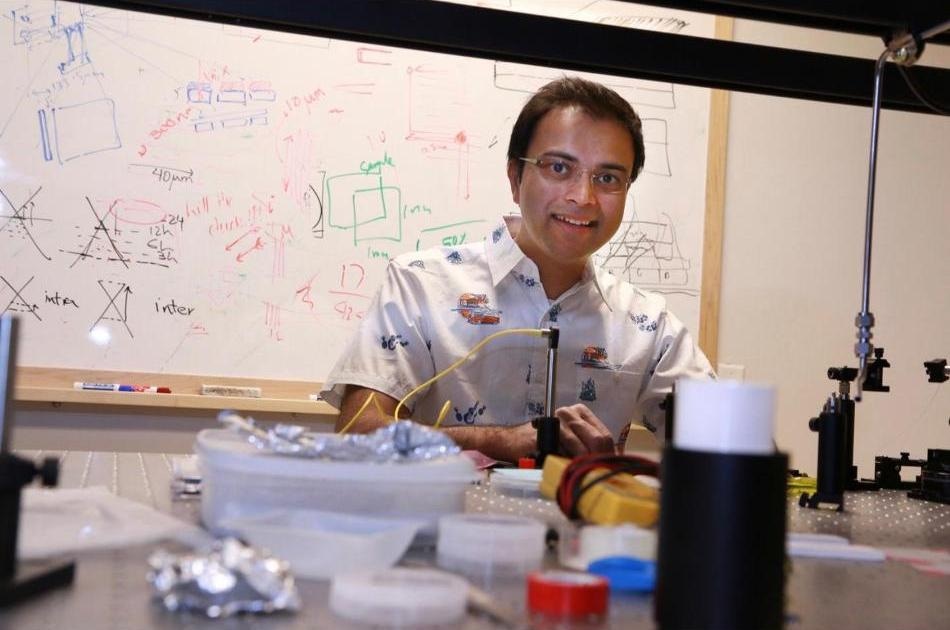
 University of Utah electrical and computer engineering associate professor Rajesh Menon (pictured) and his team have developed a cloaking device for microscopic photonic integrated devices—the building blocks of photonic computer chips that run on light instead of electrical current—in an effort to make future chips smaller, faster and consume much less power. Credit: Dan Hixson/University of Utah College of Engineering.
The fascinating power of invisibility was only the product of dreamers and science fiction writers, may it be the Romulan cloaking device in “Star Trek” that made the warship invisible, or the invisibility cloak worn by Harry Potter.
In an attempt to miniaturize future chips and to make them power-efficient and function faster, Rajesh Menon, electrical and computer engineering associate professor from the University of Utah, and his group have created a cloaking device that can be used for microscopic photonic integrated devices, which are the primary components of photonic computer chips that work on light rather than electrical current.
Menon’s findings were recently published online in the latest edition of Nature Communications. Bing Shen, a doctoral student in the University of Utah, and Randy Polson, senior optical engineer in the Utah Nanofab, were the co-authors of the article.
The future of data centers, computers and mobile devices will involve photonic chips where data is shuttled around and processed as light photons instead of electrons. Compared to the existing silicon-based chips, the photonic chips are far superior as they are comparatively very fast and utilize less power, consequently radiating less heat.
Similar to billions of transistors performing various functions in the existing silicon chips, each of the billions of photonic devices inside each photonic chip possesses a particular function. For instance, one group of devices may perform specific processing operations, another group may perform calculations, and so on.
However, the problem is that if two photonic devices are positioned closer to each other the leakage of light between the devices causes “crosstalk”, similar to radio interference, and hinders the operation of the devices. As a solution, if the devices are positioned far from each other, then this in turn causes increase in the size of the chip.
Menon and his group discovered that a custom-built barrier made of nanopatterned silicon placed between the two photonic devices functions similar to a “cloak” and prevents the devices from viewing each other.
The principle we are using is similar to that of the Harry Potter invisibility cloak. Any light that comes to one device is redirected back as if to mimic the situation of not having a neighboring device. It's like a barrier -- it pushes the light back into the original device. It is being fooled into thinking there is nothing on the other side.
Rajesh Menon, Associate Professor, University of Utah
As a result, it is possible to pack billions of these photonic devices in a single chip, increasing the functionality of the chip. As the photonic chips use light photons to transfer data rather than electrons that radiate heat, they can actually consume power that is 10 -100 times less, which would be a boon for places like data centers that consume enormous amounts of power.
Menon is highly confident that the most immediate use of this technology, and in general photonic chips, will be in data centers such as those used by Facebook and Google. As stated by the U.S. Department of Energy’s Lawrence Berkeley National Laboratory, in 2014, data centers located only in the United States used 70 billion kilowatt hours, i.e. approximately 1.8% of total power consumption in the United States. Moreover, by 2020, this electricity consumption is anticipated to increase by another 4%.
By going from electronics to photonics we can make computers much more efficient and ultimately make a big impact on carbon emissions and energy usage for all kinds of things. It's a big impact and a lot of people are trying to solve it.
Rajesh Menon, Associate Professor, University of Utah
At present, photonic devices are employed only in high-end military equipment. Menon anticipates that the usage of full photonic-based chips in data centers will commence within the next few years.