May 25 2016
Studying electrical and mechanical properties under strain provides unprecedented insights into the behaviour of thin film devices, with a new Olympus application note detailing how confocal laser scanning microscopy challenges AFM in reinventing flexible electronic design.

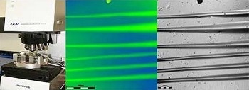
Advancing research into flexible thin film electronic devices, Dr Megan Cordill from the Erich Schmid Institute for Materials Science and the University of Leoben (Austria), has employed confocal laser scanning microscopy (CLSM) with the Olympus LEXT OLS4100. Coupling a mechanical straining stage with high-resolution observation allows in situ analysis of electrical and mechanical properties, and CLSM proved to be a faster and more insightful alternative to atomic force microscopy (AFM). Evidence generated illustrates the damaging effects promoted by the inclusion of interlayers, facilitating cutting-edge research that can be viewed in the latest Olympus application note.
The electronics industry is rapidly moving towards flexible thin film devices, but designs must withstand stress. Working towards this aim, Dr Cordill studies the behaviour of thin film devices during strain, with in situ electro-mechanical testing reflecting the strength and electrical resistance of the film, as well as its adhesion to the substrate.
Observation data generated with the LEXT OLS4100 was found to compare to that produced by the AFM, with added benefits. These included improved speed and ease of use. In addition, a larger field of view and higher range allowed more comprehensive analysis, as the AFM can only visualise shallower surface features and 4-5 cracks per image, failing to provide meaningful statistics.
Compared to AFM I would say it takes half the time to learn how to run the LEXT system. Anyone can use an AFM, but to get high quality images, you need more experience, and it can be hard to inspect the same area each time. With the LEXT it is much easier to get it right the first time, as image acquisition is straightforward and intuitive.
Dr Cordill
Shedding light on the behaviour of thin film devices, utilising the LEXT OLS4100 in Dr Cordill’s research has demonstrated how conventional designs with interlayers between the substrate and conducting thin film are detrimental. While a chromium layer between a copper film and polymer promotes cracking, the tantalum adhesion layer beneath gold films leads to buckling and delamination. With the new setup, manufacturers can determine when damage appears, and respond to this information in the drive to develop robust, market-ready devices.
Combining Olympus’ digital light microscopy technology with mechanical testing, the Olympus LEXT OLS4100 offers possibilities throughout a vast field of applications across all sectors of material science. For more information about the 3D measurement capabilities of light microscopy systems, and to view a webinar explaining Dr Cordill’s research, please visit our 3D-Measurement Website.