Apr 6 2016
Checkpoint Technologies, LLC, announces further advancements in Visible Laser Probing of Si Integrated Circuits. Checkpoint has developed a visible laser-probing module that is compatible with its InfraScan™ product family. Checkpoint’s visible laser probing leverages its industry leading LTM™ and Solid Immersion Lens - SIL technology, allowing its users to debug the latest circuit designs at the 10 nm node with the potential for utilization down to 5 nm node.
 Vis-SIL Visible Laser Probing (Graphic: Business Wire)
“This technology break through is proof that Checkpoint is leading the way in optical resolution for silicon IC debugging,” stated Michael Jupina, Checkpoint’s General Manager. “By incorporating a high speed visible detector in to the LTM with a Visible SIL, Checkpoint is giving its users unprecedented resolution and debugging power.”
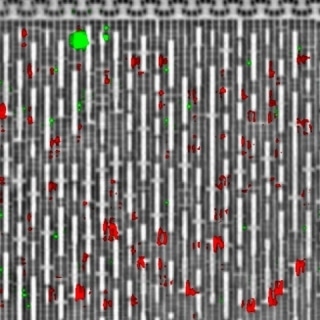
Checkpoint has demonstrated the Vis-SIL and Visible LTM on 10 nm to 16 nm circuits. The images below show clear resolution improvement, on 16 nm IC’s, compared to a near IR SIL, greater than a factor of two while maintaining signal to noise to extract clear electrical waveforms and signal mapped images (SMI’s).
Checkpoint Technologies, LLC, is a recognized leader in the failure analysis industry supplying laser scanning and photon emission microscopy systems for diagnostic purposes used by major semiconductor manufacturers.
About Checkpoint Technologies, LLC:
Founded in 1995, Checkpoint Technologies develops and manufactures optical failure analysis tools that are used by semiconductor manufacturers to improve the speed and reliability of integrated circuits. Checkpoints role is to help integrated circuit manufacturers produce more reliable and better functioning electronic devices. Checkpoint Technologies is headquartered in San Jose, California USA with worldwide sales and service.