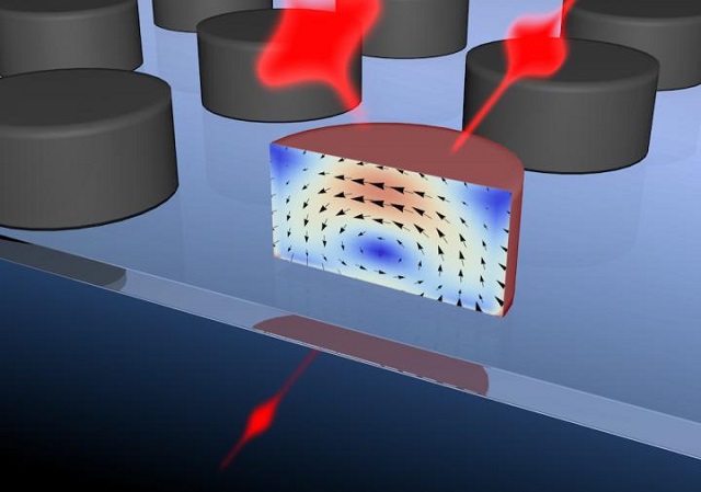
Scientists have successfully developed the world's fastest nanoscale all-optical switch. The device uses plasmonic nanoparticles and can transfer terabits of data on a femtosecond scale
 the device is a disc 250 nm in diameter that is capable of switching optical pulses at femtosecond rates (Credit: Maxim Scherbakov et al)
Produced on silicon nanostructures, the nanoscale device can be used for high-speed data transfer and may serve as a platform for next-gen computers.
The photonics field is branch of optics research that gained prominence with the invention of lasers. Photonics shares the same objectives as electronics, that is the fast, accurate and unattenuated transfer of data, but uses photons, rather than electrons, as the signal transfer agent. A photon refers to a quantum of light.
Photons do not interact with one another making them an attractive method of data transmission when compared to electrons. .In computing applications, the key feature that needs to be improved is instructions per second (IPS). The IPS is held back by the limit on electron density that is intrinsic to materials. Photons can can be packed more densely than electrons, allowing a higher IPS to be acheived.
Electronic transistors are fundamental components in modern electronic instruments. The standard scale of these electronic transistors is around 100 nm. In contrast, the standard scale of photonic transistors remains at on a few micrometers, that is 100 times the size. Plasmonic nanoparticles are nanoscale structures that can compete with electronic structures; however, these structures tend to experience major data losses and have a low efficiency. Because of this behaviour it was difficult to develop a compact all-optical switch.
However the development was made easier due to a significant phenomnenon observed by the scientists at Moscow State University. They discovered that silicon nanoparticles are characterized by magnetic dipole resonances, which are powerful resonances in the visible spectrum. The strong localization of subwavelength-scale light waves defines the magnetic dipole resonances within the nanoparticles. Maxim Shcherbakov, the chief author of the study, realised that this discovery could pave the way for developing a small and ultrafast all-optical switch.
A 250 nm-diameter device was ultimately developed that can easily switch optical pulses at femtosecond speeds. With such ultrafast switching speeds, processing devices can be created that will transmit data at several terabits per second. This means thousands of high-definition movies could be downloaded within a fraction of a second.
The all-optical switch exploits the interactions that occur between pairs of femtosecond pulses. The interaction occurs as a result of the magnetic resonance exhibited by the silicon nanostructures. When the pulses arrive simultaineously at the silicon nanostructure one of the signals is dampened because due to two-photon absorption. If there is a 100-fs delay between the two pulses no interaction occurs and the second pulse travels through the nanostructure with no change.
In our experimental research me and my colleague Polina Vabishchevich from the Faculty used a set of nonlinear optics methods that address femtosecond light-matter. We used our femtosecond laser complex acquired as part of the MSU development program.
We were able to develop a structure with the undesirable free-carrier effects are suppressed. Free carriers (electrons and electron holes) place serious restrictions on the speed of signal conversion in the traditional integrated photonics. Our work represents an important step towards novel and efficient active photonic devices-- transistors, logic units, and others. Features of the technology implemented in our work will allow its use in silicon photonics. In the nearest future, we are going to test such nanoparticles in integrated circuits.
Maxim Shcherbakov - MSU