Feb 22 2012
Nanolane of France, a specialist in the development and commercialisation of optical solutions for characterising nanomaterial systems, has launched Sarfus Mapping Lite — an innovative measurement solution that fits with any optical microscope set-up functioning with reflected light.
French-based Nanolane has recently created easy-to-use Sarfus Mapping Lite, a plug-in piece of apparatus, the main components of which are a set of Surf microscope slides, step-height standards and a powerful piece of software. Sarfus Mapping Lite fits with all optical microscopes that use reflected light. Thanks to the technology developed by Nanolane, what has remained invisible to an optical microscope for so long is now revealed clearly.

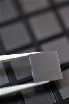
Surf slides replace ordinary microscope glass slides and are where users deposit samples. The users then handle the optical microscope as usual, apart from the fact that the contrast enhancement brought about by Surf is such that they can see nano-objects in the shape of films, tubes or particles directly through eyepieces, i.e. with the naked eye.
The data conversion software included in the Sarfus Mapping Lite package takes a Charged Coupled Device (CCD) camera-obtained 2D colour image and provides a 3D thickness map of a nanometric sample. To do so, the optical instrument, i.e. the combination of the optical microscope and colour camera, is calibrated. This calibration occurs thanks to a series of nanometric step-height standards that are traceable to the ISO 17025 standard. These standards mean that a detection limit, which can be as high as 0.1nm (instrument dependent), is guaranteed.
Up until now, Surf-slide users were able to sense and image nanometric objects, such as nanotubes, nanowires, DNA strands, and nanoparticles. With Sarfus Mapping Lite, they will also be able to measure thin films and surface treatment of items with nanometric thickness.
The benefits one gains from adding Sarfus Mapping Lite to a microscope, as compared to the current nanocharacterisation or imaging tools, are, above all, related to its excellent accessibility and user friendliness.
Real-time image acquisition makes it possible to record fast dynamic phenomena, depending on the camera’s capacities. A selectable field of view, ranging from a few µm² to several mm², depending on magnification, gives users the flexibility to study their samples globally. This global studying is useful for locating regions of interest (ROIs). The selectable field of view also allows samples to be studied locally, so as to investigate micro- to sub-micro-details. Additionally, the viewing technique is non-contact in nature and, therefore, truly non-destructive.
Applications of Sarfus Mapping Lite are many, from thin-film characterisation (for organics, inorganics, liquid crystals and lithography) to biological systems (such as biochips and biofilms), among many others. More fundamental research-related applications include nanopatterns, Langmuir-Blodgett films, and self-assembled monolayers(SAMs), for example.