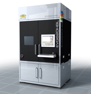
EV Group, a provider of lithography and wafer-bonding equipment, has introduced its second-generation completely automated mask alignment equipment, the EVG620HBL Gen II for mass-production of high-brightness LEDs (HB-LEDs).
 EVG620HBL Gen II
The EVG620HBL Gen II has been launched a year after the release of the first-generation EVG620HBL. It is custom designed to address the specific needs of HB-LED customers and reduces the total cost-of-ownership. It also improves the tool footprint in a fab by delivering a 55% increase in wafer output for each square meter of the cleanroom area.
The Gen II system features an improved microscope that leverages automated mask pattern search, which in turn decreases mask setup and change time in order to allow nonstop device production in high-volume manufacturing conditions. Its upgraded robotic handling layout together with wafer mapping capability facilitates the demand for wafer traceability. Its enhanced alignment capability supports the grids used for marking individual LEDs for orientation, thus eliminating the use of alignment marks that occupy considerable wafer space. Its decreased footprint increases wafer output per footprint index and improves total cost of ownership. With these key features, the EVG620HBL Gen II reduces cost per processed wafer by 20% when compared to competitive products.
The EVG620HBL series is developed on the established mask aligner platform of EV Group. Its high-intensity ultraviolet light source together with an optional filter fan unit optimizes wafer output to up to 165 numbers of 6" wafers per hour. Its special recipe-controlled microscopes’ illumination spectrum can be altered and improved to obtain the optimal pattern contrast with different wafers and layer materials such as aluminum nitride, silicon carbide, sapphire, ceramic and metal. It processes 2-6" wafers.