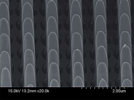
A research team led by Xiuling Li, who serves as a Professor of electrical and computer engineering at the University of Illinois at Urbana-Champaign, has developed a low-cost method to fabricate high-aspect-ratio, large-area III-V nanostructures for applications in advanced optoelectronic devices such as lasers and solar cells.
 A scanning electron microscope image of “nanopillars” etched in gallium arsenide. (Credit: Xiuling Li)
For the fabrication of the III-V nanostructures, the research team used a wet-etching method dubbed as metal-assisted chemical etching (MacEtch), which was originally designed by the team for the silicon process. Contrary to the other wet processes, MacEtch is a top-down process. According to Li, her method is low cost and quicker when compared to most of the dry etch processes.
The research team has used its MacEtch process for the III-V semiconductor gallium arsenide (GaAs) by enhancing the reaction conditions and chemical solutions. In the two-step process, the initial step is the patterning of a metal thin film over the surface of the GaAs using a patterning technique developed by John Rogers, who serves as a materials science and engineering professor at the University of Illinois at Urbana-Champaign. The patterning process dubbed as soft lithography protects the surface of the GaAs, while allowing chemical compatibility.
Now, the GaAs material comprising the metal pattern is submerged in the chemical solution of the MacEtch. A reaction is catalyzed by the metal to etch away the areas in contact with the metal, resulting in the creation of the high-aspect-ratio structures, as the metal immerses into the wafer. After the completion of the etching process, the metal can be removed from the surface without causing damage to it.
Li stated that the integration of the MacEtch process and the soft lithography process enables low-cost production of high-aspect-ratio, large-area III-V nanostructures. The research team plans to extend its research to optimize conditions for the etching process of GaAs and set parameters to process other III-V semiconductors using the MacEtch process. The team also intends to demonstrate the fabrication of devices such as photonic crystals and distributed Bragg reflector lasers.