Electron microscopy (EM) is an experimental method employed to capture high-resolution images of microscopic samples. It is a powerful technique to study the detailed structure of biological specimens such as tissues and cells.

Image Credit: Elizaveta Galitckaia/Shutterstock.com
Electron microscopes improve on the limitations of light microscopes. Historically, light microscopes were used to magnify and study the structure of organic samples. One of the major drawbacks of optical microscopes is the phenomenon of light diffraction. Light diffraction imposes a limit on how clearly a microscopic sample can be imaged.
Diffraction of Light
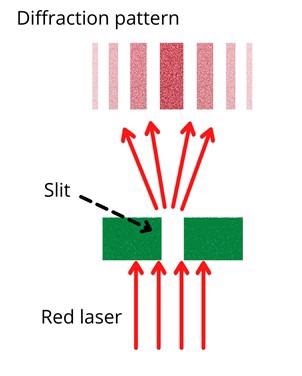
Diffraction is the bending of light as it passes through an opening or around the edge of an object. As shown in Figure 1, when light passes through an opening, it spreads out due to diffraction. Bright and dark lines are formed if the diffraction pattern is projected on a screen. These bright and dark lines are the maxima and minima points of the light rays coming together after traveling the distance from the slit to the screen.

Figure 1: Illustration of light diffraction. Image Credit: Ilamaran Sivarajah
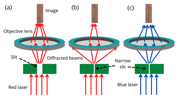
By placing a convex lens or an objective in the diffracted beam path, the image of the slit, or an object, can be formed (Figure 2a). For a sharp, clear image to be formed, the lens must be capable of capturing all the diffracted rays of light. The image will be blurred if the lens is unable to capture all the diffracted light.

Figure 2: (a) Illustration of an image formed after using a lens to capture the diffracted light. (b) When the slit or object gets smaller, the image formed gets blurry. (c) Blue laser light which is lower in wavelength than red light forms a clearer image due to less diffraction. Image Credit: Ilamaran Sivarajah
When the slit becomes smaller, the diffraction increases. The light rays fan out more as they pass through the slit. As seen in Figure 2b, less diffracted light rays are captured by the lens and the image becomes blurry.
German optical scientist Ernst Karl Abbe formulated the resolving power of an optical microscope in 1873. Abbe’s equation gives the relationship between the wavelength of light, the property of the lens, and the size of the object that can be imaged with an optical microscope.
Depending on the wavelength of light, the maximum sample size that can be imaged is 200-250 nanometers.
In the visible spectrum of light, red light exhibits the maximum diffraction due to its longer wavelength. Longer wavelength light diffracts more than shorter wavelength light. This results in images formed with red light being blurrier than images formed using UV or blue light as seen in Figure 2b and 2c.
The limitation imposed by light diffraction restricts optical microscopes from being able to produce high-resolution images of very small samples.
Wave-Particle Duality
In 1924, French physicist Louis de Broglie theorized the wave-particle duality of matter. The wave-particle duality postulates that all matter exhibits both particle and wave-like behavior.
In 1927, the wave-particle duality was experimentally verified using electron beams as a source for diffraction. When a beam of electrons, which are charged particles, was directed through a slit, a diffraction pattern was formed on a screen. But diffraction is a phenomenon that only occurs for waves. Through this experiment, the dual wave-particle behavior of electrons was demonstrated. Thus, proving de Broglie’s theory and earning him the Nobel prize in physics in 1929.
The Invention of the Electron Microscope
In 1933, German physicist Ernst Ruska built the first electron microscope. Electrons have a much lower wavelength than photons, which are particles of light. The diffraction limit imposed by the wavelength of light is lifted when electrons are used instead.
The diffraction of electron beams is collected with magnetic lenses as electrons are charged particles. Images formed with an electron microscope are 1000 times higher in resolution than optical microscopes.
There are two major types of electron microscopes: transmission electron microscope (TEM) and scanning electron microscope (SEM).
Transmission Electron Microscope (TEM)
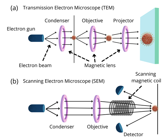
The underlying operational principle of a TEM is illustrated in Figure 3a. An electron beam source is produced by an electron gun. Since moving electrons produce magnetic fields, their beam path can be guided using electromagnetic lenses. The TEM has a condenser lens, an objective lens, and a projector lens which guide the electron beam as shown in Figure 3a.
In TEM, the samples are usually stained with uranyl acetate, which produces a high-electron density in the sample, helping to create higher image contrast.

Figure 3: Schematic diagrams of (a) Transmission Electron Microscope (TEM) and (b) Scanning Electron Microscope (SEM). Image Credit: Ilamaran Sivarajah
Scanning Electron Microscope (SEM)
SEM is a modified technique that scans the specimen and projects high-resolution images on a detector. Similar to the TEM, the SEM uses an electron gun as a source, an electromagnetic condenser, and objective lenses to guide the beam (Figure 3b).
An additional scanning coil is used in SEM instead of an objective. The scanning coil moves the electron beam in two dimensions along the coil’s plane.
The object being imaged is coated with heavy metals such as gold, platinum, or tungsten. The presence of heavy metals on the surface of the object backscatters the impacting electrons. The back-scattered electrons are collected by electron detectors and high-resolution images are constructed using software.
Electron Microscope Variations and Impact
The electron microscope was instrumental in supporting a new era of scientific discoveries, as knowledge of cell structures in plant and animal life increased remarkably.
Ernst Ruska was awarded the 1986 Nobel prize in physics for his discovery of the electron microscope. Further variations such as scanning tunneling microscopy (STM) and cryogenic electron microscopy (cryo-EM) have advanced the imaging techniques. The development of the latter also garnered a Nobel prize in chemistry in 2017.
References and Further Reading
Brodusch N, Demers H, Gauvin R. (2018) Imaging with a Commercial Electron Backscatter Diffraction (EBSD) Camera in a Scanning Electron Microscope: A Review. Journal of Imaging. 4(7):88. https://doi.org/10.3390/jimaging4070088
Aoon Rizvi, Justin T. Mulvey, Brooke P. Carpenter, Rain Talosig, and Joseph P. Patterson. (2021) A Close Look at Molecular Self-Assembly with the Transmission Electron Microscope. Chemical Reviews. 121 (22), 14232-14280 https://pubs.acs.org/doi/10.1021/acs.chemrev.1c00189
Golding, C., Lamboo, L., Beniac, D. et al. (2016) The scanning electron microscope in microbiology and diagnosis of infectious disease. Sci Rep 6, 26516. https://doi.org/10.1038/srep26516
Disclaimer: The views expressed here are those of the author expressed in their private capacity and do not necessarily represent the views of AZoM.com Limited T/A AZoNetwork the owner and operator of this website. This disclaimer forms part of the Terms and conditions of use of this website.