Jul 8 2007
In efforts that can improve studies of biological objects and the construction of nanotech materials, researchers at the University of California-Berkeley have invented "optoelectronic tweezers," a new way of controlling nanometer-scale objects.
The research will be presented at the upcoming CLEO/QELS meeting in Baltimore.
 |
|
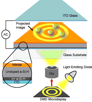
Credit: Integrated Photonics Laboratory, UC Berkeley. Principal Investigator: Ming C. Wu
Schematic of "optoelectronic tweezers."
|
In the design, the researchers reflect light from a digitally controlled array of mirrors, sending the light through a magnifying lens, and then into a sandwich of semiconductor planes, creating (at the interface between two of the planes) as many as 15,000 traps that can be addressed separately. In each of the traps, objects such as biological cells can be studied. Optoelectronic tweezers, which use optical energy to create powerful electric forces in carefully prescribed places, differ from ordinary optical tweezers, which use optical energy to create mechanical forces that can push things around, helping to make the technique potentially easier for laboratories to implement.
According to Berkeley's Aaron Ohta, the optoelectronic approach uses much less power than optical tweezers and doesn't need to be as carefully focused. In recent months the Berkeley group has had some success in using their locally controlled electric fields to manipulate the positions of tiny nanorods (100 nanometers in diameter and 1-50 microns long). The rods are suspended in a thin layer of water by sound waves and then transferred to the tweezer apparatus. Ohta says that the lateral-field optoelectronic device will possibly be used to place rods for the sake of building 3-D circuitry or for positioning oblong-shaped cells or cell protrusions with micron-level precision.