Jan 30 2010
Researchers in the Electro-Optics Center (EOC) Materials Division at Penn State have produced 100mm diameter graphene wafers, a key milestone in the development of graphene for next generation high frequency electronic devices. Graphene is a 2-dimensional layer of tightly bound carbon atoms arranged in hexagonal arrays. Sheets of graphene are the building blocks of graphite. Due to its phenomenal electronic properties, graphene has been considered as a leading material for next generation electronic devices in the multibillion dollar semiconductor industry.
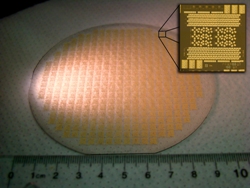
 A 100mm graphene wafer containing approximately 75,000 devices and test structures. Inset - an optical image of a single chip.
Using a process called silicon sublimation, EOC researchers David Snyder and Randy Cavalero thermally processed silicon carbide wafers in a physical vapor transport furnace until the silicon migrated away from the surface, leaving behind a layer of carbon that formed into a one- to two-atom-thick film of graphene on the wafer surface. Achieving 100mm graphene wafers has put the Penn State EOC in a leading position for the synthesis of ultra-large graphene and graphene-based devices.
With the support of the Naval Surface Warfare Center, EOC researchers are initially focusing on graphene materials to improve the transistor performance in various radio frequency (RF) applications. According to EOC materials scientist Joshua Robinson, Penn State is developing graphene device processing to enhance graphene transistor performance and has fabricated RF field effect transistors on 100mm graphene wafers.
Another goal of the Penn State researchers is to improve the electron mobility of the Si-sublimated wafers to nearer the theoretical limit, approximately 100 times faster than silicon. That will require improvements in the material quality and device design, says Robinson, but there is significant room for improvements in growth and processing, he believes.
In addition to silicon sublimation, EOC researchers Joshua Robinson, Mark Fanton, Brian Weiland, Kathleen Trumbull, and Michael LaBella are developing the synthesis and device fabrication of graphene on silicon using a non-sublimation route as a means to achieve wafer diameters exceeding 200mm, a necessity for integrating graphene into the existing semiconductor industry. Graphene has the potential to enable terahertz computing at processor speeds 100 to 1000 times faster than silicon.
First discovered in 2004, graphene is now being studied worldwide for electronics, displays, solar cells, sensors, and hydrogen storage. With its remarkable physical, chemical, and structural properties, graphene promises to become a key material for 21st century technology.
The Materials Research Institute coordinates the research of more than 200 materials scientists at Penn State. The Millennium Science Complex, now under construction, is a $225M facility for materials and life sciences research scheduled to open at University Park in summer 2011.