Dec 21 2008
Slowing light down to one-hundredth of its normal speed using photonic crystal cavities shows promise for making all-optical circuits.

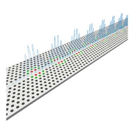
Researchers at the NTT Basic Research Laboratories in Japan have succeeded in making the first large-scale coupled nanocavities that can slow light down to one-hundredth of its normal speed. Slow light could be used in photonic memories or logic circuits, which are both difficult to make using present-day technology (Nature Photonics 2 741).
"This is the first demonstration of a large-scale array of wavelength-sized coupled cavities," team member Masaya Notomi told nanotechweb.org. "The cavities are two orders of magnitude smaller than previously coupled cavities and the cavity Q is one order of magnitude higher." Two types of velocity are used to describe the propagation of a wave in a dispersive medium: the phase velocity and the group velocity. The phase velocity is the speed at which light of a single wavelength moves.
However, a pulse of light contains a range of wavelengths that all move at different speeds, so the group velocity is defined as the speed at which the pulse itself moves. Low group velocities are beneficial for many applications because they enhance the interactions between the light and the material in a device.
Coupled cavity structures Among the different media available to reduce the speed of light, coupled cavity structures are one of the most promising. This is because their light-guiding modes theoretically exhibit slow group velocity with small group velocity dispersion, unlike many other light-slowing materials. Until now, however, the performance of real coupled cavities has been limited because it is fundamentally difficult to assemble large arrays of very small and high Q cavities.
Light speed slows down the more cavity size decreases and cavity Q becomes higher. Notomi and co-workers have exploited photonic crystals (periodically modulated nanofabricated dielectric structures) to produce high-Q coupled cavities. Photonic crystals were used because they can strongly confine light. Previous work by the team showed that a single photonic crystal cavity can exhibit a long optical delay, but coupled cavities were not made. "By employing high-resolution lithography, we succeeded in coupling 200 ultrasmall and ultrahigh-Q cavities together," explained Notomi. "The cavities can slow light down to less than c/100."
The result shows that ultraslow light elements can be extended to large scales on a chip, which suggests that all-optical processing is possible. The arrays could be used in photonic buffer memories or photonic switches that consume very little power. They will also be useful for making on-chip photonics, including memories and logic, says Notomi. The team now plans to optimise the coupled cavities and enlarge the bandwidth and delay by increasing the number of cavities. "At the same time, we will try to enhance light–matter interactions, theoretically expected in our slow light coupled cavities," added Notomi.