Metal halide perovskites have rightfully earned the status of "star" materials within semiconductors due to their outstanding optoelectronic properties. These include remarkable features such as high photoluminescence (PL) quantum yield (QY), a high absorption coefficient, tunable bandgaps, long carrier diffusion lengths, and a notable tolerance to defects.
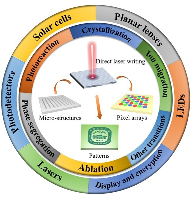 Schematic overview of direct laser writing on halide perovskites: from mechanisms to applications. Image Credit: Light: Advanced Manufacturing
Meanwhile, DLW, leveraging the interaction between light and matter, represents an efficient, contactless, mask-free, and depth-resolved micro-patterning technique. Typically, it involves coupling a laser beam with a high-resolution microscope to minimize the output focal spot. The resolution of DLW relies on both the diameter of the output focal spot and the threshold response of the material.
Depending on fabrication mechanisms and material threshold responses, optimal resolution typically ranges from a couple to a few hundred nanometers. Research on DLW also enhances the fundamental understanding of the interaction mechanisms between light and perovskites, paving the way for designing optoelectronic devices with enhanced performances.
A group of scientists led by Professor Zhixing Gan from the Center for Future Optoelectronic Functional Materials, Nanjing Normal University, China, and colleagues compiled recent DLW research progress on perovskites in a study published in Light Advanced & Manufacturing.
The concrete interaction mechanisms between lasers and perovskites are categorized into six parts: laser ablation, laser-induced crystallization, laser-induced ion migration, laser-induced phase segregation, laser-induced photoreaction, and other laser-induced transitions. Subsequently, attention shifts towards the applications of these perovskites with micro/nanopatterns and array structures, spanning areas such as displays, optical information encryption, solar cells, LEDs, lasers, photodetectors, and planar lenses.
Notably, the advantages of patterned structures are underscored. Finally, current challenges for DLW on perovskites are outlined, alongside perspectives on their future developments.
A laser is a highly effective instrument for manipulating, fabricating, and processing nano- and micro-structures on semiconductors. DLW, developed based on various interaction mechanisms between lasers and perovskites, owes its existence to the unique structure of perovskites. The intricate interaction mechanism is highly sensitive to laser parameters such as wavelength, pulse/CW, power, and repetition rate.
DLW emerges as a versatile and potent tool for precisely fabricating nano- or micro-structures in perovskites. The diverse range of interaction mechanisms underscores DLW's immense potential for microelectronics, photonics, and optoelectronics applications.
Cheaper and more flexibly controllable fabrication lasers, combined with perovskite's exceptional optoelectronic properties, promise significant application potential for DLW on perovskites. Although still in its infancy stage, there is anticipation of a substantial surge in fundamental research and industry demand in the near future.
Addressing crucial technical bottlenecks, such as DLW technique resolution, phase segregation duration, and micropatterning techniques for flexible substrates, is imperative for the future development of DLW on perovskites.
The applications of perovskites span various optoelectronic and photonic domains, including single photon sources, micro/nanolasers, photodetectors, optical gates, optical communication, waveguides, and nonlinear optics. Consequently, there is immense promise in constructing and integrating photonic devices with diverse functionalities based on a single perovskite chip.
Journal Reference:
Sheng, Y., et al. (2024) Direct laser writing on halide perovskites: from mechanisms to applications. Light: Advanced Manufacturing. doi.org/10.37188/lam.2024.004.