Augmented reality and other immersive technologies are changing how people play, observe, and learn, from pterodactyls flying above a game to digitally trying on cosmetics before making a purchase. Immersive displays could be used to their full capacity with the use of inexpensive, extremely small light-emitting diodes (LEDs), which are now unavailable.
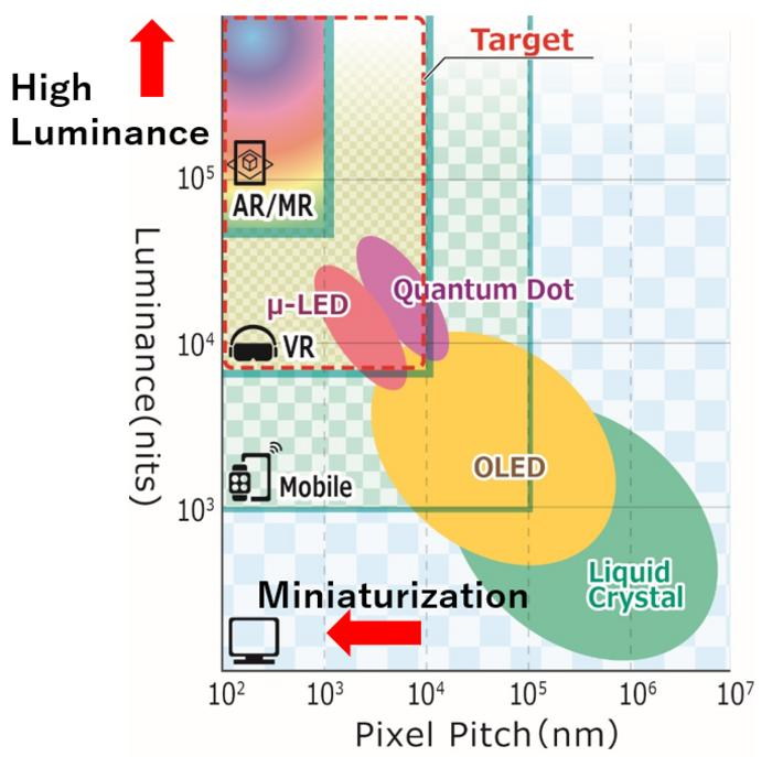
 Display Trends and Targets of This Technology. Image Credit: Motoaki Iwaya / Meijo University
Now, a group led by scientists from Meijo University and King Abdullah University of Science and Technology (KAUST) has successfully constructed such LEDs, according to a study that was just published in Applied Physics Express. These LEDs could easily be integrated into metaverse applications due to how easily they could be manufactured using already accessible manufacturing techniques.
Why is the improvement of LED technology required for immersive reality? Resolution, detail, and color breadth all affect how realistic augmented and virtual reality is. For instance, every color must be easily visible and recognizable from the others.
All of these needs are satisfied by the adaptable materials for LEDs known as gallium indium nitride semiconductors. To achieve the best performance, they must be built as a single unit on the same substrate as opposed to as individual components. The researchers intended to carry out this task.
We sequentially stacked blue, green, and red micro-LED arrays—connected by tunnel junctions, based on the quantum mechanical principle of electron transport through a thin insulating layer—onto the same wafer. We fabricated complex mesa architectures and attained a pixel density of 330 pixels per inch.
Motoaki Iwaya, Study Senior Author and Academic Researcher, Meijo University
The LEDs’ emission wavelengths were 486, 514, and 604 nanometers at a current density of 50 amperes per square centimeter, respectively. Red, blue, and green light can all be produced with the emission spectrum’s entire breadth at its half maximum, which is more than enough to discriminate between the colors.
There were a few extraneous emitted wavelengths, and the red and blue emissions were substantially less than the green emission—both attributable to damage during device fabrication. Optimizing the crystal growth conditions should ameliorate these defects.
Kazuhiro Ohkawa, Study Senior Author and Professor, King Abdullah University of Science and Technology
The common drawbacks of earlier LEDs built using gallium indium nitride technology have been reduced by this study.
Preparing the devices on cheap sapphire substrates will be necessary for practical use, and such work is underway in our laboratory. We believe our work is an important step toward realistic, immersive visual experiences that require ultra-high brightness and definition.
Daisuke Iida, Study Senior Author and Senior Research Scientist, King Abdullah University of Science and Technology
Journal Reference:
Saito, T., et al. (2023) RGB monolithic GaInN-based μLED arrays connected via tunnel junctions. Applied Physics Express. doi:10.35848/1882-0786/aced7c