Spectrometers with hetero-integration capabilities and miniaturized features are required for lab-on-chip applications such as point-of-care diagnosis, the Internet of Things, and others to acquire real-time spectral data. Solution-processable semiconductors, as opposed to traditional semiconductors integrated via heteroepitaxy, offer a far more versatile integration platform and are hence more suited for multi-material integrated systems.

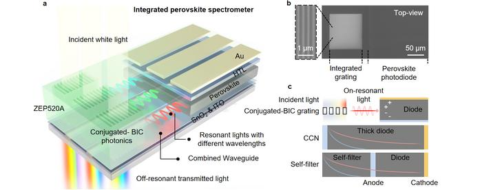
(a) The schematic working mechanism of the integrated spectrometer. Conjugated-BIC photonics and combined waveguides are planarly integrated with perovskite photodiode arrays. Monochromatic light with a specific wavelength can be coupled into the waveguide and propagate to the corresponding photodiode for an ultra-narrowband response. (b) Top-view SEM image of an ultra-narrowband photodiode that constitutes the integrated spectrometer. Zoom-in SEM image: details of the grating. (c) Schematic mechanism comparison between our mechanism (upper panel) and the conventional mechanisms (middle and lower panels). Curves represent the photocarrier density generated by lights with different wavelengths. Image Credit: Yanhao Li, Xiong Jiang, Yimu Chen, Yuhan Wang, Yunkai Wu, De Yu, Kaiyang Wang, Sai Bai, Shumin Xiao, Qinghai Song
The inability of solution-processable semiconductors to work with microfabrication techniques, however, prevents them from being used for numerous lab-on-chip applications.
Researchers from the Ministry of Industry and Information Technology Key Lab of Micro-Nano Optoelectronic Information System, Guangdong Provincial Key Laboratory of Semiconductor Optoelectronic Materials and Intelligent Photonic Systems, and Harbin Institute of Technology (Shenzhen), China, propose a simple and broad platform to fabricate integrated spectrometers with solution-processed light-emitting diodes (SPDs) in a new study published in Light: Science & Applications.
The broadband photodiodes are given ultra-narrowband detection ability, detection wavelength tunability, and on-chip integration ability while maintaining device performance by specifically utilizing the conjugated-BIC photonics, which remains untapped in standard lasing investigations.
High spectral resolution and wide/tunable spectral bandwidth are two characteristics of spectrometers built on these ultra-narrowband photodiode arrays. It is possible to expand the manufacturing procedures to conventional semiconductors by making them compatible with solution-processable semiconductor photodiodes like perovskites and quantum dots.
The incident spectra are immediately constituted by the spectrometer signals, which are not computationally demanding, latency-sensitive, or error-tolerant. For instance, integrated spectrometers based on perovskite photodiodes are capable of achieving in-situ hyperspectral imaging and narrowband/broadband light reconstruction. The published platform offers information on building integrated spectrometers with multi-material integrated systems.
The scientists stated, “Exploring the conjugated-BIC is unconventional when compared with those popular BIC lasing studies. Through the theoretical study, we find that the conjugated-BIC experiences high leakage and decent Q while it can be easily excited and coupled. Considering that the conjugated-BIC photonics can be facily fabricated and their resonant wavelengths can be effectively tuned, we anticipate that the conjugated-BIC is very suitable for wavelength-resolved photodetection applications.”
They concluded, “Solving the problems in fabricating perovskite photodiode arrays and integrating them with the conjugated-BIC photonics by micro-fabrication processes are also important since the materials and device interfaces of the devices can be easily destroyed during the processes by solvents and heat. We also believe that the photonics-optoelectronics integration platform we proposed can provide insight into broadening the functionalities and applications of the emerging solution-processable semiconductors like perovskites.”
Journal Reference
Li, Y., et al. (2023) A platform for integrated spectrometers based on solution-processable semiconductors. Light: Science & Applications. doi:10.1038/s41377-023-01231-1