Resonant optical phenomena in dielectrics and metals have boundless applications in numerous fields. The nanoscale confinement enables unmatched control of light–matter interaction at interfaces and surfaces, exploiting and governing the light flow.
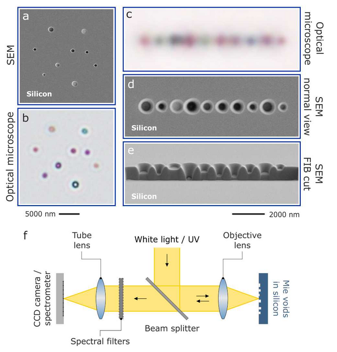
 Focused ion beam milling allows to structure conically shaped voids of varying diameter and depth into a bulk silicon wafer. (a) The scanning electron microscopy (SEM) image shows a random arrangement of holes of varying diameter and depth. (b) In the optical microscope image, one can observe the wavelength-dependent resonant scattering from the individual voids. (c) Optical microscope image. (d) Top view SEM image, (e) SEM image focused ion beam cut. (f) Sketch of the experimental setups used. The surface of the silicon is illuminated with white light and the reflected light is collected. Image Credit: M. Hentschel, K. Koshelev, F. Sterl, S. Both, J. Karst, L. Shamsafar, T. Weiss, Y. Kivshar, and H. Giessen.
Resonant phenomena are typically related to radiative and intrinsic loss channels, which are harmful in numerous systems. Metals exhibit strong intrinsic losses. Therefore, of late, dielectric technology has garnered more attention as it promises higher degrees of flexibility concerning tweaking the interplay of various resonances, lower loss, and fabrication approaches not far from industrial protocols.
In a new article reported in the journal Light Science & Application, a team of researchers, guided by Professors Harald Giessen and Mario Hentschel from the University of Stuttgart and Professor Yuri Kivshar from the Australian National University have formulated a new method for dielectric nanophotonics. This article will considerably improve antenna and structure designs.
The optical reaction of these systems is associated mainly with the exploration of optical features of high-index dielectric particles in nanophotonic devices. It is referred to as Mie theory, which develops universal building blocks for optical metasurfaces.
Mie theory is employed in the exploitation, routing, and confinement of radiation and thus initiates the beginning of the “Mie-tronic” era. However, the confinement occurs within the high-index materials. The majority of modal intensity is situated within the material. Although this is not of great concern in the near- and mid-infrared wavelength ranges, it becomes decisive for wavelength in the visible or even the UV spectral range.
The scientists experimentally execute a smooth and robust alternative route employing high-index materials. Confinement in high-index dielectrics happens because of a finite reflectance at the interface of the high-index material and air. In the case of solid particles, the mode is localized inside the high-index material. While the standard concept has been discovered earlier, these structures have not been utilized for nanophotonic applications.
The scientists demonstrated that these void modes are foreseen by Mie’s theory and possess close similarity with the Mie modes of a high-index sphere. Nonetheless, they displayed subtle but substantial differences. The uniqueness of their work is the experimental execution of a new building block. It integrates real novel functionality into the field.
They show the resonant confinement of UV radiation, detecting up to seven higher-order resonant modes in the UV. This extraordinary feature is triggered by the confinement of light in the air, enabling the whole modal volume accessible to be used and exploited. Thus far, no other resonant nanophotonic building block has been able to carry out this task.
Additional experimental work in the same direction can use other high-index materials, the mixture of Mie voids and spheres, and metallic plasmonic systems with dielectric ones. Mie voids are also predominantly applicable for optical sensing and trapping experiments and can employ chiral structures.
Mie voids could also be employed in hybrid systems where quantum emitters can be coupled to the Mie voids, which serve as local nanoantennae. It should function well in the blue and UV range. Mie voids also are especially useful in reprogrammable structures, switching, and active exploitation owing to the option of filling the mode volume in the void with dielectrics or polymers.
Journal Reference:
Hentschel, M., et al. (2023) Dielectric Mie voids: confining light in air. Light Science & Applications. doi.org/10.1038/s41377-022-01015-z.