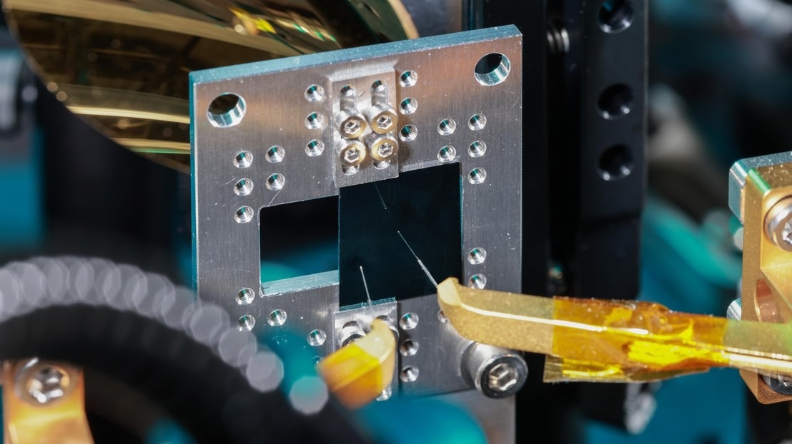
Scientists from École polytechnique fédérale de Lausanne (EPFL) have formed a partnership with those at Harvard and ETH Zurich. The collaboration is focused on a new thin-film circuit that, when connected to a laser beam, helps generate finely customizable terahertz-frequency waves.

Image Credit: © Alain Herzog
The device has given numerous opportunities for possible applications in the field of optics and telecommunications.
Scientists headed by Cristina Benea-Chelmus in the Laboratory of Hybrid Photonics (HYLAB) in EPFL’s School of Engineering have taken a major step toward successful exploitation of the alleged terahertz gap, which lies from around 300 to 30,000 gigahertz (0.3 to 30 THz) on the electromagnetic spectrum.
At present, this range is something of a technological dead zone, demonstrating frequencies that are really fast for electronics and telecommunications devices available currently. However, it is exceptionally slow for optics and imaging applications.
Currently, as a result of an extremely thin chip with a combined photonic circuit made of lithium niobate, the HYLAB scientists as well as collaborators at ETH Zurich and Harvard University have been successful not just in generating terahertz waves, but also in coming up with a solution for custom-tailoring their wavelength, frequency, phase, and amplitude.
Such accurate control over terahertz radiation implies that it can right now possibly be controlled for next-generation applications in both the optical and electronic realms. The study outcomes have been recently reported in the Nature Communications journal.
Seeing the devices emit radiation with properties that we predefined was a confirmation that our model was correct.
Alexa Herter, Study Co-First Author and PhD Student, ETH Zurich
“This was made possible due to the unique features of lithium niobate integrated photonics,” added co-first author Amirhassan Shams-Ansari, a postdoctoral fellow at Harvard University.
Telecoms-Ready
Benea-Chelmus describes the fact that while such terahertz waves have been generated in a laboratory setting before, previous methods have been dependent mainly on heavy crystals to produce the correct frequencies.
Benea-Chelmus’s laboratory use of the lithium niobate circuit, which has been finely etched at the nanometer scale by collaborators at Harvard University, makes their novel method much more simplified. Also, the use of a silicon substrate makes the device ideal for incorporation into optical and electronic systems.
Generating waves at very high frequencies is extremely challenging, and there are very few techniques that can generate them with unique patterns. We are now able to engineer the exact temporal shape of terahertz waves – to say essentially, ‘I want a waveform that looks like this.
Cristina Benea-Chelmus, Laboratory of Hybrid Photonics, School of Engineering, École polytechnique fédérale de Lausanne
For this to be achieved, Benea-Chelmus’ laboratory developed the chip’s arrangement of channels known as waveguides. This is the place from which microscopic antennas tend to broadcast terahertz waves produced by light from optical fibers.
The fact that our device already makes use of a standard optical signal is really an advantage, because it means that these new chips can be used with traditional lasers, which work very well and are very well understood. It means our device is telecommunications-compatible.
Cristina Benea-Chelmus, Laboratory of Hybrid Photonics, School of Engineering, École polytechnique fédérale de Lausanne
She sums up that miniaturized devices that transmit and receive signals in the terahertz range could play a vital role in sixth-generation mobile systems (6G).
In a world filled with optics, Benea-Chelmus notices specific potential for miniaturized lithium niobate chips in imaging and spectroscopy. Besides being non-ionizing, terahertz waves exhibit much lower energy compared to several other kinds of waves (like X-Rays) utilized at present to offer information regarding the material’s composition.
Thus, a small, non-destructive device like the lithium niobate chip could offer a less invasive alternative to present spectrographic methods.
Benea-Chelmus added, “You could imagine sending terahertz radiation through a material you are interested in and analyzing it to measure the response of the material, depending on its molecular structure. All this from a device smaller than a match head.”
Quantum Future
Subsequently, Benea-Chelmus plans to concentrate on refining the properties of the waveguides and antennas of the chip to engineer waveforms exhibiting greater amplitudes and more delicately tuned frequencies and decay rates.
Also, Chelmus notices the potential for the terahertz technology that has been developed in her laboratory to be valuable for quantum applications.
Benea-Chelmus stated, “There are many fundamental questions to address; for example, we are interested in whether we can use such chips to generate new types of quantum radiation that can be manipulated on extremely short timescales. Such waves in quantum science can be used to control quantum objects.”
Journal Reference:
Herter, A., et al. (2022) Terahertz waveform synthesis in integrated thin-film lithium niobate platform. Nature Communications. doi.org/10.1038/s41467-022-35517-6.