A lithography technique called peripheral photoinhibition (PPI) direct laser writing (DLW) is used to create complex 3D nanostructures that are frequently used in photonics and electronics. PPI-DLW employs two beams: one to excite the substrate and promote polymerization, while the other inhibits and quenches the excitation at the margins.
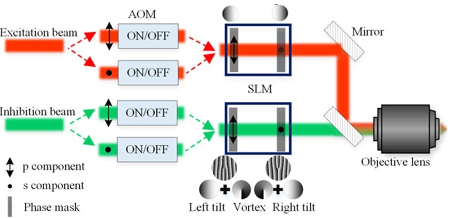
 The parallel peripheral-photoinhibition lithography system comprises eight modules arranged to allow the individual control of the split excitation and inhibition beams, thereby allowing the high-resolution, high-efficiency fabrication of nanostructures. Image Credit: Zhu et al.
The capacity is restricted in some systems, which can be enhanced using multifocal arrays. However, computing these beams requires both time and memory.
A group of Zhejiang University researchers has created a parallel peripheral-photoinhibition lithography (P3L) system capable of improved efficiency nanoscale production. Their findings were reported in Advanced Photonics.
The P3L system uses two channels, which allows the execution of different printing tasks and permits the system to fabricate highly complex structures with different periodicities.
Xu Liu, Study Senior Author, Zhejiang University
The P3L system includes a physical arrangement of eight modules. The device begins with two printing channels, consisting of an excitation solid spot and a doughnut-shaped inhibitory beam. The two beams are stabilized first and then divided into two sub-beams by a polarization filter. This enables individual control of each sub-beam via an acoustic-optical modulator.
The two sub-beams are then recombined to reestablish the excitation and inhibition beams. Spatial light modulators are then used to modulate the beams. Ultimately, the two beams are merged and sent through a microscope, where they focus as two spots on the substrate.
The individual management of each sub-beam enables the printing of nonperiodic and complicated patterns simultaneously without sacrificing scanning speed, boosting the system’s efficiency. It is simple to change the position and separation of the two spots. These characteristics make the suggested system more versatile and functional than traditional systems with uniform focus control.
The researchers proved the viability and promise of the method by producing a range of nanostructures. They began by creating a 2D sub-40 nm nanowire. A suspended nanowire with a thickness of less than 20 nm was also created. The researchers then printed dots 200 nm apart to produce two rows of alphabet patterns.
Finally, they created 3D structures with a remarkable resolution, such as nonperiodic cubic frames, hexagonal grids, wire structures, and spherical architectures.
The identical on-off control of each focus enhances the system's versatility and permits the quick production of complex, nonperiodic patterns and structures. The system's parallel scanning feature also decreases the time necessary to produce large-scale, complex structures and patterns. Regardless of whether the structure is uniform or complex, the new P3L system enables lithography efficiency twice that of current systems.
Multifocus parallel scanning and PPI have the ability to overcome the current challenges in DLW optical fabrication and enhance the fabrication of blazed gratings, microlens arrays, microfluidic structures, and metasurfaces. The proposed system could, furthermore, facilitate the realization of portable, high-resolution, high-throughput DLW.
Xu Liu, Study Senior Author, Zhejiang University
These findings make it abundantly evident that the proposed P3L system will be a valuable tool for advancing a wide range of nanotechnology-related industries.
Journal Reference
Zhu, D., et al. (2022) Direct laser writing breaking diffraction barrier based on two-focus parallel peripheral-photoinhibition lithography. Advanced Photonics. doi.org/10.1117/1.AP.4.6.066002.