Reviewed by Emily Henderson, B.Sc.Nov 8 2022
A light-based method for local material processing has been devised by researchers from the LP3 Laboratory in France that can be used anywhere in the three-dimensional region of semiconductor chips. Adding new functionalities directly with a laser makes it possible to use the subsurface area for higher integration densities and additional features.
 When intense light from ultrafast lasers is focused inside a semiconductor, highly efficient nonlinear ionization along the beam path creates an opaque plasma that prevents reaching enough energy localization near focus for material writing. Researchers from French National Center for Scientific Research (CNRS, LP3 lab.) found a new solution to this important engineering problem.
Semiconductors are still the primary component of the electronics used in modern gadgets like smartphones, automobiles, robots, and numerous other intelligent devices. The pressure on the current semiconductor manufacturing technologies is rising due to the ongoing need for powerful and miniaturized devices.
Due to the nature of these issues’ surface processing, the dominant manufacturing technology, lithography, has significant restrictions on how well it can handle them. So that the entire area inside the materials could be utilized, the development of a method to build structures beneath the wafer surfaces would be highly desirable.
The LP3 researchers present their most recent study in the International Journal of Extreme Manufacturing and show new skills to build embedded structures inside different semiconductor materials.
They successfully fabricated Si and GaAs, two crucial materials for the microelectronics industry that cannot be treated in three dimensions using traditional ultrafast lasers.
The correct wavelength selection is necessary for the light to pass through the semiconductor material. To make semiconductors a fully transparent material for this research, the wavelength is in the infrared, which is quite similar to those utilized for telecommunication applications.
The team has been working tirelessly to broaden the current range of laser processing to a wider range from UV to infrared and even longer wavelengths as part of the European Horizon project “Extreme-Light Seeded Control of Ultrafast Laser Material Modifications.”
In this study, it was conclusively established that the common telecommunication or so-called SWIR wavelengths were excellent candidates for 3D processing inside semiconductors.
There are still certain physical restrictions to overcome even after the technical problem of the proper wavelength has been resolved. Intense light is used to treat materials, which causes very effective nonlinear ionization inside narrow-gap materials to produce free electrons.
This prevents light from propagating deep inside the matter by rapidly converting semiconductors into materials resembling metal. This change impairs the focusing procedure and stops material modification with ultrafast lasers from functioning.
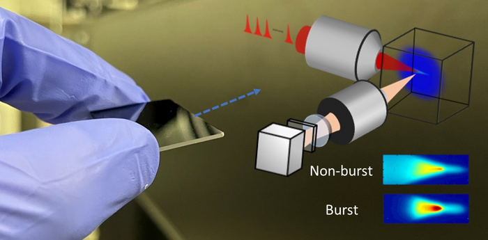
To solve this issue, the researchers suggested using unconventional ultrafast bursts of pulses to avoid the metallization transition.
Previous research used too strong light pulses that were exciting the electrons too easily. Here, instead of using strong light pulses, we split the pulse energy into a large number of weaker pulses with an extremely fast repetition rate. These pulse trains, also named bursts, will avoid strong pulse excitation before the light is focused. Additionally, the pulses will repeat very fast so that the delivered laser energy can accumulate efficiently to cross the modification.
Dr. Andong Wang, Study Investigator and Postdoctoral Researcher, LP3 Laboratory
Dr. David Grojo, who led the team, commented, “This offers the first very practical solution for ultrafast laser writing inside semiconductors. The next step will be to concentrate on the type of modifications that can be achieved inside these materials. Refractive index engineering is surely an important target given the growing importance of silicon photonics.”
He further stated, “Laser writing would offer the possibility of direct digital fabrication of 3D architecture materials inaccessible by current manufacturing technologies. In the future, these new laser modalities may drastically change the way advanced micro-chips are today fabricated.”
Journal Reference:
Wang, A. et al. (2022) Burst mode enabled ultrafast laser inscription inside gallium arsenide. International Journal of Extreme Manufacturing. doi:10.1088/2631-7990/ac8fc3