Research efforts undertaken by the group led by Professor Yanli Zhao at the Wuhan National Laboratory for Optoelectronics, Huazhong University of Science and Technology have shown that the InGaAs/Si avalanche photodiode based on a silicon on insulator substrate can be improved by using a photon-trapping structure for the first time. Their results are published in the journal Sensors.

Study: Photon-Trapping Microstructure for InGaAs/Si Avalanche Photodiodes Operating at 1.31 μm. Image Credit: atdigit/Shutterstock.com
High sensitivity avalanche photodetectors (APDs) are becoming more and more crucial in optical communication as advancements in optical networking infrastructure rapidly expand. Optical communication links are utilized in data centers to manage increased capacity data traffic and bandwidth.
Avalanche Photodetectors (APDs)
Most current APD technology is based on Group III-V materials. Group III-V materials, such as InGaAs/InP, are materials that depending on external factors or chemical changes, can function as an electrical conductor or insulator.
InGaAs/InP APD are constrained by their excess noise and bandwidth performance due to their higher ratio of impact ionization coefficients.
Ge and Si materials have lower electron mobility and lower absorption in the optical communication window than that of III-V compounds. These advantages make APD devices based on InGaAs/Si or Ge more effective for optical links.
InGaAs materials were traditionally grown on Si via epitaxy. But using this method was inefficient due to the material's large dislocations and defects. A more effective technique to create an InGaAs/Si APD with better performance is to bond the InGaAs material to the Si material to create a new InGaAs/Si heterojunction material.
Apart from improved fabrication routes, recent research has focused heavily on improving the light absorption of photodetectors using the resonant cavity effect or light-trapping structures. Previous research efforts had designed and tested a unique resonant cavity-enhanced photodetector (RCE-PD). By etching micro- and nano-holes, also known as a "photon-trapping" (PT) structure, Si photodetectors with intrinsic layer thicknesses of less than 2 meters have seen an order of magnitude improvement in their absorption efficiency. With additional optimization, this efficiency might reach more than 70%.
The team has studied an InGaAs/Si APD improved by the PT structure. Their novel design is built with the optical simulation model used for stack structure by Wanhua Zheng et al.

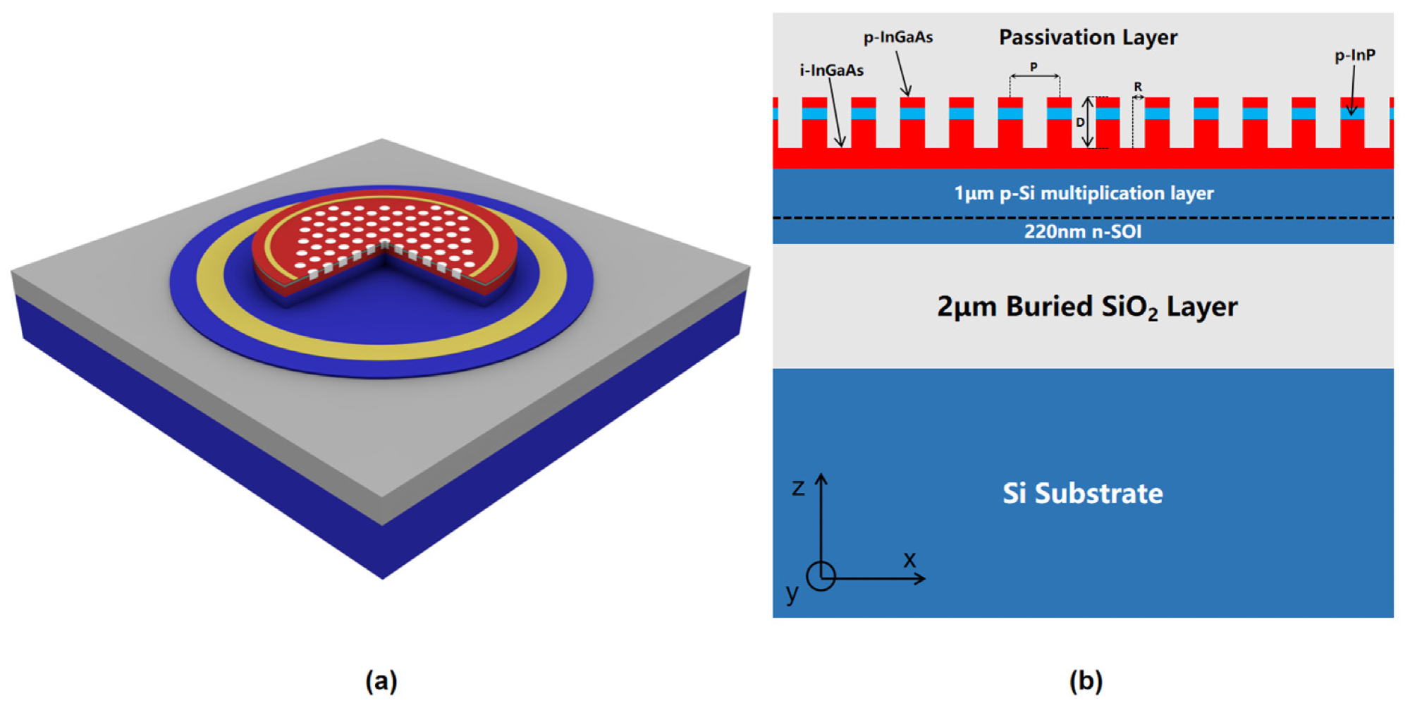
(a) 3D schematic of InGaAs/Si PT-APD; (b) cross-sectional diagram of the InGaAs/Si PT-APD.
Experimental Details
A unique InGaAs/Si photon-trapping APD (PT-APD) detector was devised with a photon-trapping nano-hole array topology to improve responsiveness. The PT structure is a square lattice with periodic nano-holes in the device's core. The distribution of the light field in the device can be changed by altering the PT-structure features, such as the depth, period, and diameter of the holes. The PT structure is built on a vertical InGaAs-Si APD. To provide the required high-refractive-index difference to restrict photons in the detector's active layer, the substrate uses a silicon on insulator (SOI) wafer.
Fabrication methods of the PT-APD and the underlying theory of the photon-trapping structure is described in detail in the publication.
The design of a highly responsive InGaAs/Si APD at the 1310 nanometer wavelength is the main objective of this work. The period of the PT structure is first optimized in the design process. The channeling mode is created in the PT structure when the period is shorter than the incident wavelength, and the development of the channeling mode is helpful in enhancing the optical coupling between the incident light and the model.
By simultaneously scanning the hole radius and hole depth, the absorption efficiency of InGaAs/Si APD with the PT structure was simulated in order to further increase the absorption efficiency of PT-APD.
The Poynting light energy distribution in particular orientations was also investigated to assess the device's optical process
To evaluate the electrical characteristics that an InGaAs/Si APD should have, electrical simulations for the stacked arrangement were performed. The results showed that the internal electric field distribution is entirely different with and without light illumination.
The improved InGaAs/Si APD's simulated dark current, photocurrent, and responsiveness were also tested as a function of the bias voltage.
Comments and Outlook
Professor Zhao’s group created a PT structure coupled with an InGaAs/Si APD based on an SOI wafer that can achieve greater responsiveness in the linear operation mode. An improved absorption, grading, charge, and multiplication-InGaAs/Si APD were proposed to enable the device's use in the optical communication sector. By adjusting the PT-structure parameters, the PT-absorption APD's performance could be significantly improved.
For standard operating voltage, the responsiveness could be increased by 1.6 times. This study investigated a brand-new technical viability for very sensitive, minimally noisy optical communication systems.
References
Zhang, H., Tian, Y., Li, Q., Ding, W., Yu, X., Lin, Z., Feng, X. and Zhao, Y., (2022) Photon-Trapping Microstructure for InGaAs/Si Avalanche Photodiodes Operating at 1.31 μm. Sensors, 22(20), p.7724. https://doi.org/10.3390/s22207724
Peng, H., Qu, H. and Zheng, W., (2020) A promising low noise and high gain InGaAs/Si avalanche photodiode. AOPC 2020: Optoelectronics and Nanophotonics; and Quantum Information Technology,. https://doi.org/10.1117/12.2579756
Disclaimer: The views expressed here are those of the author expressed in their private capacity and do not necessarily represent the views of AZoM.com Limited T/A AZoNetwork the owner and operator of this website. This disclaimer forms part of the Terms and conditions of use of this website.