Optical lens advancement has long been regarded as a significant indicator of human scientific progress. Eyeglasses, cameras, telescopes, and microscopes have all enabled us to see the world in a new light, both literally and metaphorically. Lenses are also an important part of the semiconductor industry’s nanoelectronics manufacturing process.
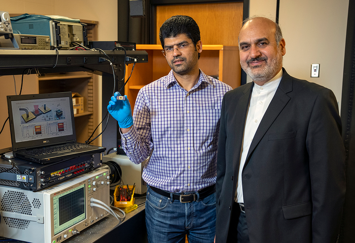
 Georgia Tech professor Ali Adibi with Ph.D. candidate Sajjad Abdollahramezani in Ali’s Photonics Research Group lab where the characterization of the tunable metasurfaces takes place. Image Credit: Georgia Tech.
The advancement of photonic metasurfaces — artificially designed nano-scale materials with spectacular optical properties — has become one of the most significant advances in lens technology in recent history. Georgia Tech scientists at the frontline of this technology revealed the first-ever electrically tunable photonic metasurface platform. The study was published in the journal Nature Communications.
Metasurfaces can make the optical systems very thin, and as they become easier to control and tune, you’ll soon find them in cell phone cameras and similar electronic imaging systems.
Ali Adibi, Professor, School of Electrical and Computer Engineering, Georgia Institute of Technology
The novel platform’s pronounced tuning measures represent a significant step forward in the development of miniaturized reconfigurable metasurfaces. The study’s findings revealed an unprecedented 11-fold change in reflective properties, a wide range of spectral tuning for operation, and a significantly faster tuning speed.
Heating Up Metasurfaces
Metasurfaces are a type of nanophotonic material in which a large number of miniaturized elements have been engineered to regulate the transmission and reflection of light at various frequencies.
When viewing under very strong microscopes, metasurfaces look like a periodic array of posts. The best analogy would be to think of a LEGO pattern formed by connecting many similar LEGO bricks next to each other.
Ali Adibi, Professor, School of Electrical and Computer Engineering, Georgia Institute of Technology
Metasurfaces have been used to show the impact of very thin optical devices on light propagation since their inception, with metalenses (the creation of thin lenses) being by far the most established application.
Despite their remarkable gains, the majority of demonstrated metasurfaces are passive, which means that their performance cannot be altered (or tuned) after manufacturing.
Adibi and his group, headed by Ph.D. candidate Sajjad Abdollahramezani, applied electrical heat to a special class of nanophotonic materials to create a platform that allows reconfigurable metasurfaces with high levels of optical modulation to be easily manufactured.
PCMs Provide the Answer
Metals, oxides, and semiconductors can all be used to make metasurfaces, but Abdollahramezani and Adibi’s research concentrates on phase-change materials (PCMs) because they can make the most effective structures with the smallest feature sizes. PCMs are materials that absorb and release heat during the heating and cooling process.
As they go from one crystallization state to another during the thermal cycling process, they are called “phase-change” materials. The most common example is water changing from a liquid to a solid or gas.
The experiments conducted by the Georgia Tech team are far more complex than simply heating and freezing water. Knowing that local heating can change the optical properties of PCMs, they have maximized the potential of the PCM alloy Ge2Sb2Te5 (GST), which is made up of antimony, germanium, and tellurium.
The group can alter the crystalline phase of the GST by merging the optical design with a miniaturized electrical microheater underneath, allowing for active tuning of the metasurface device.
The reconfigurable metasurfaces were developed at Georgia Tech’s Institute for Electronics and Nanotechnology (IEN) and tested in characterization labs by illuminating the reconfigurable metasurfaces with laser light at different frequencies and evaluating the properties of the reflected light in real-time.
What Tunable Metasurfaces Mean for the Future
Metasurfaces are quickly replacing bulky optical assemblies due to device miniaturization and system integration, and also their potential to selectively reflect different colors of light. It is expected to have an immediate impact on technologies such as LiDAR systems for imaging, autonomous cars, spectroscopy, and sensing.
According to Abdollahramezani and Adibi, more aggressive applications such as augmented reality, computing, photonic chips for artificial intelligence, and biohazard detection can be envisioned with further development.
As the platform continues to develop, reconfigurable metasurfaces will be found everywhere. They will even empower smaller endoscopes to go deep inside the body for better imaging and help medical sensors detect different biomarkers in blood.
Ali Adibi, Professor, School of Electrical and Computer Engineering, Georgia Institute of Technology
The National Science Foundation (NSF) funded this research through Grant No. 1837021. The Office of Naval Research (ONR) (N00014-18-1-2055, Dr. B. Bennett) and the Defense Advanced Research Projects Agency funded the majority of the work (D19AC00001, Dr. R. Chandrasekar). W.C. thanks ONR (N00014-17-1-2555) and the National Science Foundation (NSF) for their support (DMR-2004749).
A. Alù thanks the Air Force Office of Scientific Research and the Simons Foundation for their support. M.W. thanks the Deutsche Forschungsgemeinschaft for their support (SFB 917). NSF-CHE provided financial support to M.E.S. (1608801).
Part of this work was done at Georgia Tech’s Institute for Electronics and Nanotechnology (IEN), which is part of the National Nanotechnology Coordinated Infrastructure (NNCI), which is funded by the National Science Foundation (ECCS1542174).
Journal Reference:
Abdollahramezani, S., et al. (2022) Electrically driven reprogrammable phase-change metasurface reaching 80% efficiency. Nature Communications. doi.org/10.1038/s41467-022-29374-6.