Reviewed by Alex SmithApr 5 2022
A team of Cornell University engineers has built a deep-ultraviolet laser made up of semiconductor materials that demonstrates immense promise for enhancing the use of ultraviolet (UV) light for sanitizing water, sensing unsafe gases, sterilizing medical tools, facilitating precision photolithography and so on.
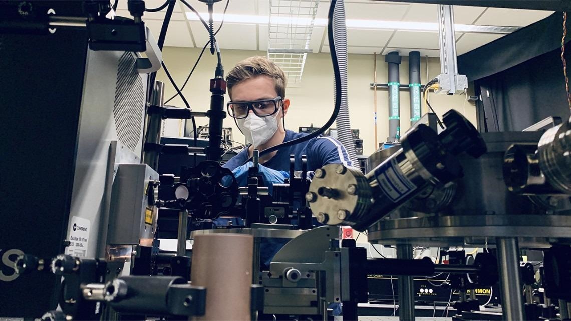
 Doctoral student Len van Deurzen works with a lab setup used to operate a deep-ultraviolet laser-emitting device. Image Credit: Cornell University
With regard to UV light, two crucial qualities are frequency — some frequencies are ideal for killing viruses or sensing molecules — and linewidth, a measure of the precision of a laser. Researchers and engineers look for sources of superior quality and better UV light emission, but it is tough to work with the semiconductor materials that can facilitate this.
An article appearing in the March 11th issue of the journal AIP Advances illustrates how Cornell researchers created an aluminum gallium nitride-based device that can emit a deep-ultraviolet laser at preferred wavelengths and modal linewidths.
It is known that this is a material that is suitable, but it was a materials synthesis problem. The challenge is making the materials pure enough that they're actually going to be useful and sustain the requirements of a laser.
Len van Deurzen, Study Lead and Doctoral Student in Applied and Engineering Physics, Cornell University
Van Deurzen took up the challenge during the COVID-19 pandemic when the market started demanding UV LEDs and other tools that can detect and eliminate the SARS-CoV-2 virus.
I wanted a research project that could have impact and the pandemic really amplified the need for improved ultraviolet devices.
Len van Deurzen, Study Lead and Doctoral Student in Applied and Engineering Physics, Cornell University
Under the direction of the article’s senior authors, Debdeep Jena and Huili Grace Xing, both professors of materials science and engineering and of electrical and computer engineering, the team used molecular beam epitaxy, a crystal growth method, to grow a superior quality crystal of aluminum nitride.
We need multiple aluminum gallium nitride layers stacked on top of each other and one important parameter is the interface quality between those layers. We can grow very sharp interfaces without the impurities and dislocations that form with other growth techniques.
Len van Deurzen, Study Lead and Doctoral Student in Applied and Engineering Physics, Cornell University
The second challenge was to develop an optical cavity from the stacked layers that could be used to capture the discharged light and boost stimulated emission, which is required for the laser. The cavity was produced in the form of a compact, micron-scale resonator on an aluminum nitride chip that van Deurzen was able to create with the assistance of the Cornell NanoScale Science and Technology Facility.
“It is a real privilege to be able to grow the materials and produce the chip at two state-of-the-art facilities located in the same building,” said van Deurzen, referring to Duffield Hall. “You just go from the third floor to the basement.”
Upon completion, the laser could accomplish peak gain at a wavelength of 284 nm and modal linewidths on the order of 0.1 nm. The linewidth is an order of magnitude more exact than comparable devices and shows the growth process’ applicability toward better UV light emitters.
The deep-ultraviolet laser made by the Cornell team is optically pumped, that is, it creates certain requirements for lasing by adding photons into the device. The following step in the study, according to Jena, is employing the same materials platform to attain a laser that is powered by an electrical current from a battery — a more real-world energy source for light-emitting devices available in the market.
Deep-ultraviolet lasers arguably are the final frontier in semiconductor materials and devices with immense long-term payoffs. Yet it is also the kind of problem that a young graduate student can get into and make an immediate impact.
Debdeep Jena, Study Senior Author, the David E. Burr Professor of Engineering and the Richard E. Lunquist Sesquicentennial Faculty Fellow, Cornell University
The co-authors of the study include doctoral student Ryan Page and research associates Kazuki Nomoto and Vladimir Protasenko. The study was sponsored by the U.S. Department of Energy and was supported by user facilities financially backed by the National Science Foundation.
Journal Reference:
Van Deurzen, L., et al. (2022) Optically pumped deep-UV multimode lasing in AlGaN double heterostructure grown by molecular beam homoepitaxy. AIP Advances. doi.org/10.1063/5.0085365.