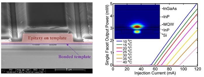
A new study led by researchers Yingtao Hu, Di Liang and Raymond G. Beausoleil from Hewlett Packard Labs, Hewlett Packard Enterprise, Milpitas, CA, USA, discusses advanced III-V-on-silicon photonic integration.
 SEM image of a fabricated device by using epitaxial regrowth on bonded template and measured LI curves of the device. Image Credit: OEA.
The study has been published as a new review article in the journal Opto-Electronic Advances.
Integrating various materials to enjoy their benefits concurrently and even achieve new functionalities is always desirable in different fields, from food to fashion, to semiconductor industries.
Silicon photonics aids the combination of III-V optical gain materials onto a silicon substrate to attain an on-chip light source. Among several integration techniques, heterogeneously combining III-V material onto a silicon substrate with the help of wafer bonding technology is the most well-known and is presently appearing in commercial products.
At the same time, direct epitaxial growth of III-V layers on silicon also has great research interest as a result of its ability as a solution for very high-density integration over a long period. Besides the above-mentioned III-V-on-silicon photonic integration methods, a new III-V-on-silicon photonic integration method that involves epitaxial regrowth of III-V material on a bonded substrate has attracted a great deal of interest.
Research teams from Hewlett Packard Labs, III-V labs, and Sophia University have invested in this latest integration method and illustrated their working lasers individually. By making a native template on silicon substrate with the help of wafer bonding technology, lattice-matched epitaxy can be carried out consequently on the template.
The aim of this latest integration method is to offer high-quality III-V-on-silicon photonic integration by profit from both direct epitaxy and wafer bonding technologies.
In this study, scientists from Hewlett Packard Labs (considered one of the chief research forces in this topic) review new research work on this integration platform of regrowth on a bonded template from several research teams.
Thanks to the analyses of the similarities and variations of template developments, comparisons and analysis of the epitaxial regrowth and fabricated laser devices, there has been increasing interest and huge potential in this novel concept of regrowth on bonded template.
Additional discussions have shown that this technique has several potential benefits, for example, it offers high-quality laser material on Si substrate and is competitively priced over other existing III-V-on-silicon integration methods.
Specifically, besides the huge practicality for the on-chip light source and other functional devices for Si photonics, scientists from Hewlett Packard Labs consider that this integration idea is a general method for integrating diverse materials onto various substrates.
This integration platform is expected to be employed in low-cost, high-scalability and high integration density photonic integration applications and to an even wider area for sophisticated material combinations.
Journal Reference:
Hu, Y., et al. (2021) An advanced III-V-on-silicon photonic integration platform. Opto-Electronic Advances. doi.org/10.29026/oea.2021.200094.