Jun 12 2020
Camera lenses could be considerably less resource-intensive to manufacture and thousands of times thinner in the years to come.
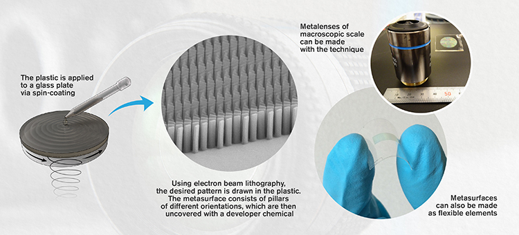
 Ultra-thin and flexible “metalenses” could eventually replace traditional camera lenses. Researchers at Chalmers now present a new and more resource-efficient way to make metasurfaces—artificial materials made of nanoparticles—using plastic. Image Credit: Daniel Andrén and Yen Strandqvist.
At the Chalmers University of Technology, scientists have currently developed a new technology for creating artificial materials called “metasurfaces,” which include a multitude of interacting nanoparticles that can control light when combined. They could be used extensively in next-generation optical technology.
Metasurfaces can be utilized for optical components in cameras, portable electronics, space satellites, or sensors. The new technology developed by the Chalmers scientists to create these planar surfaces relies on a plastic that is already in use to make other microstructures.
We put a thin layer of this plastic on a glass plate and, using a well-established technique called electron-beam lithography, we can draw detailed patterns in the plastic film, which after development will constitute the metasurface. The resulting device can focus light just like a normal camera lens, but it is thousands of times thinner—and can be flexible too.
Daniel Andrén, PhD Student, Department of Physics, Chalmers University of Technology
Andrén is also the first author of the paper recently published in the ACS Photonics journal.
In the past decade, the field of optics has undergone a major revolution. Present-day smartphones have cameras similar to a DSLR—technological masterpieces with a resolution of millions of pixels. They process light using small cutting-edge computer chips and software, and the image is reconstructed using small colored LEDs.
In recent years, such technologies have developed very rapidly, thanks to smaller and more effective circuit components.
But camera lenses have not been altered much. Most of the existing lenses are based on similar physical principles and suffer from the same fundamental restrictions as the initial prototypes that were developed in the 16th century.
However, in the last 10 years, scientists have started to work with artificial materials—metasurfaces—that could serve as alternatives to the existing lenses.
At present, some problems hinder the large-scale production of metasurfaces. Most sophisticated equipment is needed to manufacture them, and the process also takes plenty of time.
However, through the new technique developed by the Chalmers scientists, the rate of production can be ramped up multiple times than the existing advanced methods. The new technology involves using safe chemicals and machines that are already common in nano-manufacturing laboratories, which implies that more scientists can now start analyzing metasurfaces.
Our method could be a step towards large-scale production of metasurfaces. That is the goal we are already working towards today. Metasurfaces can help us create different effects and offer various technological possibilities. The best is yet to come.
Ruggero Verre, Researcher, Department of Physics, Chalmers University of Technology
Verre is also a co-author of the study.
Journal Reference:
Andrén, D., et al. (2020) Large-Scale Metasurfaces Made by an Exposed Resist. ACS Photonics. doi.org/10.1021/acsphotonics.9b01809.