Apr 16 2020
Although the use of extreme ultraviolet light sources to develop sophisticated integrated chips has been in the pipeline, their advancement has been hampered due to a lack of efficient laser targets.

Image Credit: Keiji Nagai
At the Tokyo Institute of Technology (Tokyo Tech), researchers recently created a very low-density tin “bubble,” which renders the generation of extreme ultraviolet cost-effective and reliable. This innovative technology opens the door for several applications in electronics and looks promising for the fields of cancer therapy and biotechnology.
For developing next-generation devices, their core—named the integrated circuit chip—should be more compact and efficient than those currently available. To manufacture these chips, robust light sources are needed. Recently, the use of extreme ultraviolet (EUV, an extremely short-wavelength radiation) range light sources has gained considerable attention. However, these light sources are difficult to produce.
One solution is to use high-intensity lasers: recent developments in laser technology have resulted in the development of lasers with lower cost and higher power. High-intensity lasers achieve laser plasmas, and their first practical use is the production of EUV light to develop semiconductor integrated circuits. During this process, the lasers illuminate a suitable “target,” and consequently, a high-density and high-temperature state is formed.
A 13.5 nm light with high brightness is produced from this state, which can be employed to manufacture the integrated chips. However, this task is not simple, as it has been challenging to control the target density that can generate light in the EUV range. Although researchers have considered tin as an option, its development has been hampered due to the failure to control its dynamics.
For this purpose, a research team, including Associate Professor Keiji Nagai from Tokyo Tech and Assistant Professor Christopher Musgrave from University College, Dublin, endeavored to find efficient laser targets.
An innovative type of low-density material, which is inexpensive and scalable, has been described in a study reported in Scientific Reports. According to Prof Nagai, “EUV light has become crucial in today's world but is expensive owing to the high-volume manufacturing.”
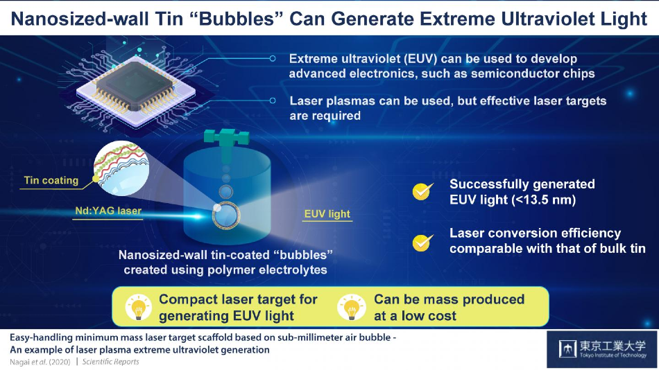
The researchers started by developing a tin-coated microcapsule or “bubble,” which is an extremely low-density structure that weighs as low as 4.2 ng. They achieved this by using polymer electrolytes (salts dissolved in a polymer matrix), which serve as surfactants to stabilize the bubbles. Then, tin nanoparticles were used to coat the bubbles.
We produced polyelectrolyte microcapsules composed of poly(sodium 4-styrene-sulfonate) and poly(allylamine hydrochloride) and then coated them in a tin oxide nanoparticle solution.
Keiji Nagai, Associate Professor, Tokyo Institute of Technology
The researchers tested the use of this bubble by irradiating it with a neodymium-YAG laser. This led to the production of EUV light, which falls within the 13.5 nm range. The team even identified that the structure was compatible with traditional EUV light sources used to develop semiconductor chips.
However, a major benefit was that, while using the tin bubble, the laser conversion efficiency—a measure of the laser power—matched that of bulk tin.
Overcoming the limitations of liquid tin dynamics can be very advantageous in generating EUV light. Well-defined low-density tin targets can support a wide range of materials including their shape, pore size, density etc.
Keiji Nagai, Associate Professor, Tokyo Institute of Technology
Over several years, Prof. Nagai and his colleagues have created a number of low-density materials for laser targets. However, their efforts were hampered by problems with mass productivity and manufacturing costs. At present, the integration of new low-density tin targets formed of bubbles is an appealing solution for the mass production of a compact 13.5 nm light source at a lower cost.
Apart from finding uses in electronics, Prof Nagai believes that their innovative technology comprising “bubble” laser targets could even be applied to cancer therapy.
This method could be utilized as a potential small scale/compact EUV source, and future quantum beam sources such as electrons, ions, and x-rays by changing the coating to other elements.
Keiji Nagai, Associate Professor, Tokyo Institute of Technology
Prof Nagai and his colleagues intend to partner with large laser facilities in Japan and overseas for further studies.