Jan 6 2020
A metalens can be defined as a thin composite metal-dielectric film positioned on a dielectric substrate. It measures several dozen nanometers in width. The metalens has been described in the latest article featured in Optics Letters.
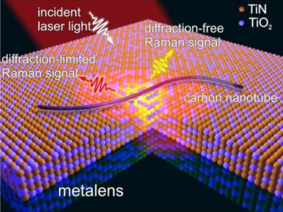
 Schematic of the working principle of a disordered TiN∕TiO2 metalens. Image Credit: Kazan Federal University.
The study was funded by a Russian Science Foundation’s grant under the title “Synthesis and research of a new class of nanocomposite ceramics with degenerate dielectric permeability for opto-plasmonic applications.”
The light has a wave nature, so there is a diffraction limit which confines the resolution of traditional optical microscopy. Our metalens is an optical device capable of surpassing that diffraction limit. Such a solution paves way for using optical technologies in nanoscale integral circuits and sensors.
Dr Sergey Kharintsev, Researcher, Kazan Federal University
Such an ultra-high resolution is built on an extraordinary behavior of the metalens in infrared and optical ranges.
Kharintsev continued, “The material part of the dielectric constant oscillates near zero. This property can be used to enhance stimulated Raman scattering of light in a spatially limited medium illuminated by low-intensity continuous laser light.
“For most materials found in nature, nonlinear effects are weak, and to observe them it is necessary to increase the length of the medium (for example, using optical fibers) and/or to increase the laser pump power (using high-power pulsed lasers), Kharintsev added.
We used a 50 nm thick titanium oxynitride (TiON) film as a disordered nonlinear medium. The film was synthesized by magnetron sputtering and subsequent oxidation in air. As a result of a two-stage procedure, metal (TiN) and dielectric (TiO2) nanoparticles were formed in the film. An increase in the amplitude of the Stokes wave in a TiN/TiO2 film occurs due to the enhancement of the cubic susceptibility because of localized plasmon resonance and a small refractive index of the effective medium.
Dr Sergey Kharintsev, Researcher, Kazan Federal University
Kharintsev further added, “Such metal-insulator nanocomposite films having several epsilon-near-zero frequencies in the visible and infrared ranges have found application in creating broadband metal technologies providing resolution beyond the limits of light diffraction.”
The employees at Kazan University have successfully observed 40-nm multiwall carbon nanotubes that were distributed along the surface of the metalens developed. The resolution of this metalens was found to be less than 100 nm.
Nanocomposite epsilon-near-zero film works as a surface-enhanced Raman scattering substrate, and it helps not only enhance the scattered signal, but also achieve beyond-diffraction resolutions. Metalenses and ENZ films can be used to create broadband absorbers for solar panels.
Dr Sergey Kharintsev, Researcher, Kazan Federal University