Aug 5 2019
A new study has revealed that atomically thin semiconductors produce light at a lower voltage when they are integrated together in a LEGO style. This breakthrough discovery may result in low-energy consumption devices.
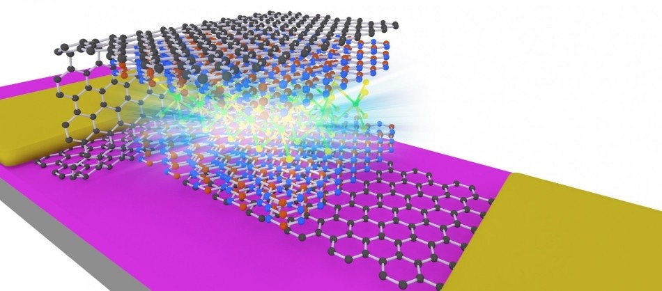
 (Image credit: The University of Manchester)
Although the study is still in its fundamental state, this shows potential for practical applications in telecommunications and optoelectronics.
An LED’s voltage is often equivalent to or larger than the bandgap energy for each electron charge. Now, a research team from The University of Manchester, the High Magnetic Field Laboratory in Grenoble, the University of Warsaw, and the National Institute for Materials Science in Japan has successfully demonstrated LEDs that switch on at relatively lower voltages.
The concept to stack layers of varied materials to make the so-called heterostructures dates back to the 1960s, when semiconductor gallium arsenide was studied for fabricating tiny lasers—which are extensively being utilized.
Currently, heterostructures are quite common and are used much widely in the semiconductor sector as a tool for designing and controlling optical and electronic characteristics in devices.
New kinds of heterostructures have evolved more recently in the period of atomically thin two-dimensional (2D) crystals, like graphene. Atomically thin layers in those heterostructures are held together by comparatively weak van der Waals forces.
The novel structures dubbed “van der Waals heterostructures” could pave the way for producing innovative devices and many designer-materials by arranging any number of atomically thin layers together. An unlimited number of combinations become feasible that otherwise cannot be accessed in conventional three-dimensional (3D) materials, possibly providing access to exotic characteristics of materials or new unexplored functionality of optoelectronic devices.
Numerous research teams in the world have carried out a large number of experiments, which concentrate on light-emitting characteristics of transition metal dichalcogenides. But, most often, such studies are performed mainly through optical methods. Electrically activated light emission is more preferred for practical applications. The study results have been reported in Nature Communications.
The research team, headed by Dr Aleksey Kozikov, Professor Marek Potemski, and Professor Kostya Novoselov, used electricity to do this. The researchers initially bound holes and electrons sitting in varied transition metal dichalcogenides—the so-called interlayer excitons. They then produced experimental conditions when these interlayer excitons reintegrate non-radiatively, referred to as Auger effect.
The discharged energy is transmitted to other charge carriers that can subsequently shift to higher energy states. Consequently, charge carriers whose energy was initially very low to overcome the bandgap of the material, can now effortlessly cross this potential barrier, reintegrate, and produce light. This effect is known as upconversion.
With the help of graphene electrodes, charge carriers were electrically injected via hexagonal boron nitride arranged in a heterostructure within tungsten diselenide (WSe2) and molybdenum disulfide (MoS2). The distance between these transition metal dichalcogenides can be changed by adding boron nitride in between them. This helps in adjusting the LEDs from a regular operation to a low-voltage operation and visualizing the effect of upconversion.
From the central standpoint, the visualized effects represent a significant step towards the realization of superfluidity of van der Waals heterostructures and exciton condensation.
When we started measuring the first MoS2/WSe2 devices we were really surprised to observe emission at such low applied voltages. This upconverted emission impressively shows the importance of Auger processes for interlayer excitons in van der Waals heterostructures. Our findings shed more light on the physics in the largely unexplored high carrier density regime, which is crucial for optoelectronic applications as well as for fundamental phenomena like interlayer exciton condensation.
Dr Johannes Binder, Study First Author, University of Warsaw
Dr Aleksey Kozikov added, “it is fascinating how adding just one atomically thin material can change properties of a device so dramatically. This is the power of van der Waals heterostructures in action.”