Apr 16 2019
Usually, atoms or molecules are created when particles bond in free space. However, it is possible to create even more exotic bonding states inside solid objects.
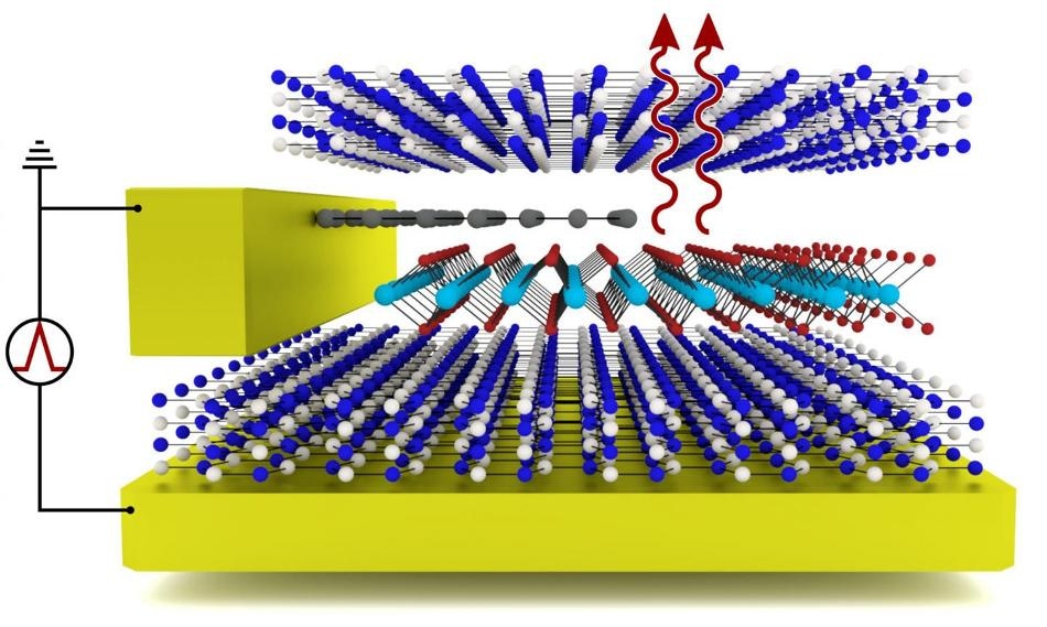
 Short electric pulses are sent through a system of ultrathin layers, which then emits light. (Image credit: TU Wien)
Presently, scientists at TU Wien have succeeded in leveraging this: what are called as “multi-particle exciton complexes” have been created by the application of electrical pulses to very thin layers of material composed of tungsten and sulfur or selenium.
These exciton clusters are bonding states composed of electrons and “holes” in the material and can be transformed into light. The outcome is a new type of light-emitting diode in which the wavelength of the preferred light can be controlled with high precision. These findings have now been reported in the journal Nature Communications.
Electrons and Holes
Electrical charge can be carried in two different methods in a semiconductor material. On one hand, electrons can travel straight through the material from atom to atom where they carry negative charge with them. On the other hand, if an electron is absent somewhere in the semiconductor, that point will be positively charged and known as a “hole.” If an electron moves from an adjacent atom and fills the hole, it in turn creates a hole in its previous site. In this way, holes can travel across the material in the same way as electrons but in the opposite direction.
Under certain circumstances, holes and electrons can bond to each other. Similar to how an electron orbits the positively charged atomic nucleus in a hydrogen atom, an electron can orbit the positively charged hole in a solid object.
Prof. Thomas Mueller, Photonics Institute, Faculty of Electrical Engineering and Information Technology, TU Wien
Much more complex bonding states are possible: so-called trions, quintons, or biexcitons which have three, four, or five bonding partners. “For example, the biexciton is the exciton equivalent of the hydrogen molecule H2,” describes Thomas Mueller.
Two-Dimensional Layers
In the majority of solids, such bonding states are only possible at very low temperatures. However, this is not the case with so-called “two-dimensional materials,” which only comprise of atom-thin layers. The group at TU Wien, whose members also included Matthias Paur and Aday Molina-Mendoza, has developed an ingeniously designed sandwich structure in which a thin layer of tungsten disulfide or tungsten diselenide is placed in between two boron nitride layers. Using graphene electrodes, an electrical charge can be applied to this ultra-thin layer system.
“The excitons have a much higher bonding energy in two-dimensional layered systems than in conventional solids and are therefore considerably more stable. Simple bonding states consisting of electrons and holes can be demonstrated even at room temperature. Large, exciton complexes can be detected at low temperatures,” states Thomas Mueller.
Based on how the system is supplied with electrical energy using short voltage pulses, different excitons complexes can be created. When these complexes decay, they emit energy in the form of light which is how the newly developed layer system operates as a light-emitting diode.
Our luminous layer system not only represents a great opportunity to study excitons, but is also an innovative light source. We therefore now have a light-emitting diode whose wavelength can be specifically influenced—and very easily too, simply via changing the shape of the electrical pulse applied.
Matthias Paur, Study Lead Author, TU Wien