Apr 3 2019
ICFO scientists have developed an extremely sensitive CMOS compatible broadband photodetector by modifying material defects.
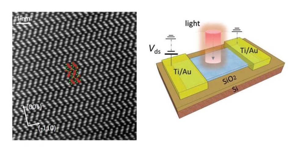
 Left: STEM imaging of crystal where the red and green balls represent bismuth and sulfur atoms. Right: Schematic illustration of Bi2S3 detector on the Si/SiO2 substrate. (Image credit: ICFO)
There has been a pressing need in consumer electronics for infrared optoelectronics such as LEDS and photodetectors. Up to now, however, infrared optoelectronics are served by expensive CMOS incompatible III-V semiconductors. Lately, a new group of semiconductors that address the CMOS compatibility matter have been developed founded on colloidal quantum dots. With regards to consumer electronics, the use of RoHS-compliant materials is a precondition and hence there is a robust need for the advancement of high performance devices grounded on environmentally friendly elements, a concept that in the infrared had remained intangible.
To look into this challenge ICFO scientists have learned that by manipulating flaws in materials one can lengthen the semiconductor’s spectral reach well over its bandgap, expanding, by this means, the availability of material for the infrared part of the spectrum.
In a new research published in Advanced Optical Materials, ICFO scientists Dr. Nengjie Huo, Dr. Alberto Figueroba, Dr. Y. Yang, Dr. Sotirios Christodoulou, Dr. Alexandros Stavrinadis, led by ICREA Prof at ICFO Gerasimos Konstantatos, in partnership with Prof. C. Magén from Univ. of Zaragoza, have reported on the creation of an infrared detector using bismuth sulfide, which has been established to be fast and have high photo-response levels in the short-wave infrared range on account of the formation of defects in the material. In their experiment, the team of scientists produced a photoconductive detector, placing a very thin layer of Bi2S3 flakes onto a Si/SiO2 substrate. Once constructed, the team was able to see that the Bi2S3 flakes contained sulfur vacancies or flaws in the material (sulfur-deficient), which formed extended in-gap states, which allowed more absorption of light below the bandgap value of Bi2S3 that is sub-bandgap. Such features resulted in a high gain, low noise and, then, a high sensitivity photodetector.
To gain insights in the sulfur deficiency mechanism, they constructed a second photodetector and synthesized the Bi2S3 crystal, by carrying out a sulfurization process (altering the concentration percentages of Bi and S in the crystal) and then refilling the sulfur vacancies. In doing this, they were able to see that the photodetector had a lot faster reaction time but was restricted to the spectral range in the near infrared. Thus, to enhance the reaction time without forfeiting its spectral coverage into the infrared, they performed a mild chemical treatment on the sulfur-deficient-based detector, via a surface passivation process of the crystal. Upon finishing the treatment, they noticed that the time reaction had reached a value of approximately 10 ms for the infrared and visible light range, 50 times quicker than the original sulfur deficient-based detector.
The results of this research offer new understandings into the role played by atomic vacancies in the electronic structure and how sub-bandgap photoresponse effects can facilitate ultrasensitive, rapid, and broadband photodetectors.
This research has been partly aided by the European Commission’s Graphene Flagship initiative.