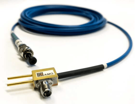
Researchers at AMO GmbH have used Oxford Instruments Plasma Technology’s fabrication solutions to develop a graphene based photonics device capable of operating at a data rate of 25 Gb/s per channel. These devices convert optical modulation data into an electrical signal that can be interpreted by today’s IT systems. They have the potential to become key enablers for next generation mobile communications unlocking data streams at ultrafast speeds with wide bandwidths.

We live in an age where data plays a pivotal role in every decision making process. Advancements in Big Data and Internet of Things (IOT) technologies that are seamlessly connecting humans to information are driving development of long range data centres with kilometres of data links. Keeping up with these ever increasing demands will require development of faster and more efficient data links. Devices developed by scientists at AMO GmbH, a non-profit SME based in Aachen, within the European Graphene Flagship project have certainly set the yard stick in terms of high speed photodetectors operating at telecom wavelengths. At the mobile world congress in Barcelona this year, AMO scientists along with collaborators with the Graphene Flagship project demonstrated the world’s first graphene data communication link operating at 25 Gbits/s per channel. As such the detector developed at AMO can reach speeds of up to 130 GHz
“We are extremely delighted to see the progress made by researchers at AMO on our device fabrication solutions”, says Frazer Anderson, Innovation and Solutions Director, Oxford Instruments Plasma Technology. He continued:” We continue to invest in further developing and improving our cutting edge device fabrication processes for datacomms and photonics through feedback from such impressive success stories”

Prof. Max Lemme, Managing Director, AMO GmbH comments: “The latest results on high-speed graphene-based data communication are very encouraging. They are a positive testament to AMO’s mission: to identify new materials and to demonstrate new technologies for future applications in electronics and optoelectronics, such as IOT and 5G. We can only achieve such results through our state-of-the-art R&D process line, which includes a large number of tools for scalable nanotechnologies, such as Oxford
Instruments’ RIE, ALD and CVD tools”
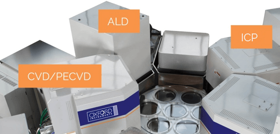
The devices were developed at AMO’s 6” device fabrication pilot line equipped with Oxford Instrument fabrication solutions which includes ICP RIE, ALD and PECVD tools. Oxford Instruments offers reliable and high performance solutions for the data communications market sector for both scaled-up production as well as novel device R&D. The detector fabrication solution includes: waveguide fabrication, III-V/2D materials mesa etching and graphene/2D/novel materials deposition. In addition Oxford Instruments also offers a range of solutions for devices such as the InP edge emitting lasers and VCSELs that are also key components of photonic data communications.