Apr 11 2018
In the recent past, femtosecond laser direct writing has been regarded as a propitious technique for the fabrication of photonic integrated chips specifically because of its intrinsic potential for three-dimensional (3D) prototyping in transparent substrates.
At present, the major setback in developing compact photonic integrated circuits (PICs) is the challenge of inducing large refractive index changes to be smoothly spread out in the laser-irradiated regions. Lately, scientists in China have come up with a solution to curb the bend loss of the waveguide at small radii of curvatures by over one order of magnitude, thereby paving the way for reducing the size of 3D photonic integrated circuits.
Their study, titled “Suppression of bend loss in writing of three-dimensional optical waveguides with femtosecond laser pulses,” was reported in the latest issue of the Science China Physics, Mechanics & Astronomy journal.
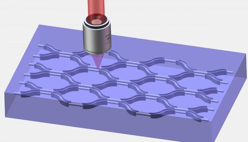
 Scheme diagram of writing compact PICs with low bend loss using a femtosecond laser. (Image credit: Science China Press)
PICs fabricated by using sophisticated photolithographic technologies are being widely used in biophotonics, optical signal processing, optical communications, and sensing applications. As an intrinsically planar fabrication technology, increasing the integration density during photolithography is chiefly dependent on decreasing the sizes of individual components. Instead, at present, PICs with geometrically complicated 3D configurations can be produced by the application of femtosecond laser direct writing, which prospectively offers exceptional flexibility and high integration density with regard to integrated multifunctional systems such as optomechanics and optofluidics.
At present, it has been demonstrated that waveguides inscribed in fused silica glass support single-mode transmission with lower propagation losses of 0.1 dB/cm at a wavelength of 1550 nm. However, the typical increase in refractive index induced in fused silica by femtosecond laser irradiation is of the order of ~10-4 to ~10-3, resulting in large bending losses at small radii of curvatures. This has transformed into a significant barrier in manufacturing compact photonic devices using the 3D waveguides written by femtosecond laser pulses.
In order to overcome this difficulty, the scientists inscribed multiple modification tracks in fused silica with the help of femtosecond laser direct writing, where the tracks were arranged into two arrays to form a pair of vertical modification walls on both sides of the curved waveguide. The modified structures result in a strongly localized densification of the material and also considerably improved structural stress in the guiding region. Consequently, the contrast in refractive index at the waveguide bend considerably increased. The bend loss of curved waveguides with a bending radius of 15 mm was successfully reduced from ~3 dB to ~0.3 dB by optimizing the geometrical parameters of the bend-loss-suppression walls (BLSWs).
Since small radii of curvatures benefit large-scale integration of PICs on a single chip, it is expected that the technique can be highly valuable for construction of chip-based photonic devices.
Dr. Yongfeng Lu, the Past President of Laser Institute of America & Lott Distinguished Professor - The University of Nebraska-Lincoln
The Major Program of National Natural Science Foundation of China (Grant No. 61590934), the Project of Shanghai Committee of Science and Technology (Grant No. 17JC1400400), and the National Basic Research Program of China (Grant No. 2014CB921303) funded this study.