Mar 10 2017
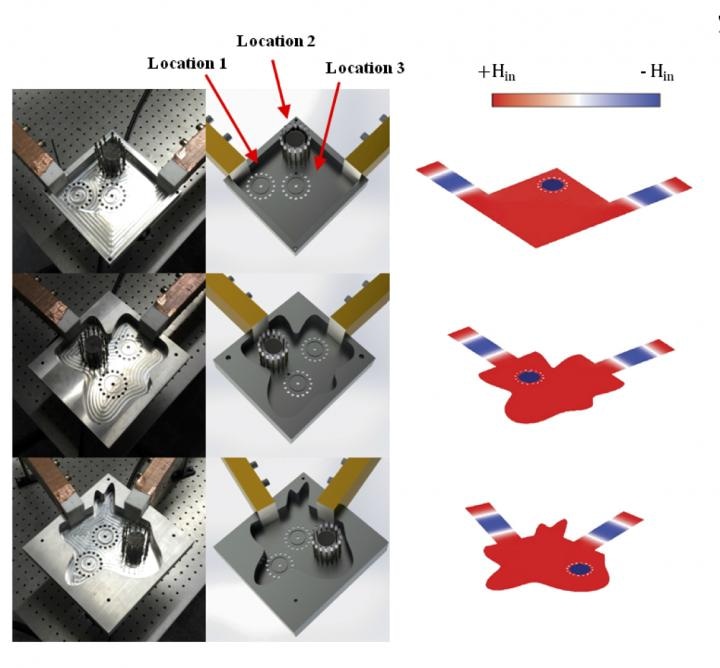
 "Physical experiments showed that the location of the dielectric rod and the shape of the ENZ material did not effect the properties of the resulting metamaterial." Credit: University of Pennsylvania
The field of metamaterials is a combination of electrical engineering, nanotechnology, physics and materials science. This field aims at producing structures with unique electromagnetic properties.
The cautious combination of several materials in an accurate periodic arrangement results in metamaterials exhibiting properties that do not otherwise exist, such as a negative index of refraction. A few metamaterials are even capable of channeling electromagnetic waves around their surfaces, causing them to be invisible for specific wavelengths of light.
The accuracy needed to assemble a metamaterial's constitutive parts, also called inclusions, has been a complex step in their application and development.
Engineers from the University of Pennsylvania have recently demonstrated a way to develop metamaterials comprising of a single inclusion, providing effortless fabrication, among various other useful features.
Analogous to electronic "doping," where including a minimum amount of atomic impurities to a "pure" material provides it electronic properties required for several sensing and computational devices, this "photonic doping" would permit for new methods of sculpting and customizing light-matter interactions, with potential impact on optical technology, such as flexible photonics.
Nader Engheta and H. Nedwill Ramsey, Professor of Electrical and Systems Engineering, headed this research together with group members Iñigo Liberal, Ahmed M. Mahmoud, Yue Li and Brian Edwards. This research has been published in the journal Science.
Just as in electronic doping, when adding a set of foreign atoms in an otherwise pure material can significantly alter the electronic and optical properties of the host, 'photonic doping' means adding a foreign photonic object in a specialized photonic host structure can change the optical scattering of the original structure in a major way.
Nader Engheta, Professor, University of Pennsylvania
The phenomenon works with a particular class of materials comprising of permittivity, which is a parameter dealing with the material’s electric response, mathematically represented by the Greek letter epsilon, that is almost zero.
One significant quality of these epsilon-near-zero (ENZ) materials is that the magnetic field of the wave is uniformly distributed all over the two-dimensional ENZ hosts, in spite of their cross-sectional shape. Such ENZ materials can be developed by standard metamaterial means or can be made naturally.
Instead of using engineer complicated periodic structures that bring about vital changes in the magnetic and optical properties of such materials, Engheta and his team worked out a way for a single inclusion in a 2-D ENZ structure in order to achieve the same task: altering which wavelengths of light that will pass through or reflect, or changing the structure’s magnetic response.
If I want to change the way a piece of material interacts with light, I normally have to change all of it. Not here. If I place a single dielectric rod anywhere within this ENZ material, the entire structure will look different from the perspective of an external wave.
Nader Engheta, Professor, University of Pennsylvania
The dielectric rod refers to a cylindrical structure produced from an insulating material capable of being polarized. When placed in a 2D ENZ host, this material will be able to affect the magnetic field within the host and will thus bring about a change in the optical properties of the host ENZ material.
It is possible to place the dielectric rod anywhere within the material as the magnetic field of the wave in the 2-D ENZ host has a uniform spatial distribution. Incoming waves act as if the host material has a considerably different set of optical properties. Such photonically doped structures can be constructed in a relatively effortless manner since the rod need not be placed at a precise location.
Employing these metamaterial concepts through "photonic doping" has applications within telecommunications and implications for information processing systems.
When we're working with a wave, this photonic doping can be a new way for us to determine the path this wave takes from A to B within a device. With a relatively small change in the dielectric rod, we can make waves 'go this way' and 'don't go that way.' That we only need to make a change to the rod, which is a tiny part of the host material, should help with the speed of the device, and, because the effect is the same for the ENZ host with arbitrary shape while keeping its cross-sectional area fixed, this property may be very useful for flexible photonics.
Nader Engheta, Professor, University of Pennsylvania
Additional research demonstrates several complicated ways of employing photonic doping to ENZ materials, such as adding numerous rods to varied diameters.
"The dielectric property of the rod can be responsive to thermal, optical or electrical changes," Engheta said. "That means we could use the host ENZ material as the read-out of a sensor, as it would transmit or reflect light due to changes in that rod. Adding more rods would allow for even finer tuning of the material's response."
The study was partially supported by the Vannevar Bush Faculty Fellow Award through Office of Naval Research grant N00014-16-1-2029, the Air Force Office of Scientific Research through Multidisciplinary University Research Initiative awards FA9550-12-1-0488 and FA9550-14-1-0389 and the National Natural Science Foundation of China through grant 61301001.