Nov 29 2016
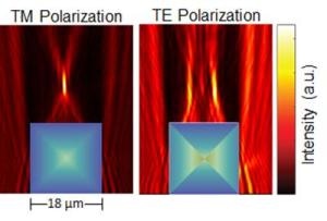
 Figure shows how the PSi square GRIN microlens focuses and splits TM and TE polarized light, respectively. TM polarized light is focused to one point and TE polarized light is focused to two different points. The refractive index gradient for the square microlens under the two different polarizations is illustrated using the color map overlaid on the lens (blue is low refractive index, and orange is high refractive index). Credit: University of Illinois
A novel approach for fabricating three-dimensional micro-optics through the shape-defined formation of porous silicon (PSi) has been developed by a multi-institutional research collaboration. This new approach has broad impacts in integrated optoelectronics, photovoltaics, and imaging.
Researchers at the University of Illinois at Urbana-Champaign collaborated with colleagues at Stanford and The Dow Chemical Company to fabricate 3D birefringent gradient refractive index (GRIN) micro-optics by electrochemically etching preformed Si micro-structures, such as square columns, PSi structures with defined refractive index profiles.
The emergence and growth of transformation optics over the past decade has revitalized interest in using GRIN optics to control light propagation. In this work, we have figured out how to couple the starting shape of the silicon micro-structure and the etch conditions to realize a unique set of desirable optical qualities. For example, these elements exhibit novel polarization-dependent optical functions, including splitting and focusing, expanding the use of PSi for a wide range of integrated photonics applications. The key is that the optical properties are a function of the etch current. If you change the etch current, you change the refractive index. We also think that the fact that we can create the structures in silicon is important, as silicon is important for photovoltaic, imaging, and integrated optics applications.
Paul Braun, Ivan Racheff Professor of Materials Science and Engineering, University of Illinois
“Our demonstration using a three-dimensional, lithographically-defined silicon platform not only displayed the power of GRIN optics, but it also illustrated it in a promising form factor and material for integration within photonic integrated circuits,” stated Neil Krueger, a former PhD student in Braun’s research group and first author of the paper, “Porous Silicon Gradient Refractive Index Micro-Optics,” appearing in Nano Letters (DOI: 10.1021/acs.nanolett.6b02939).
“The real novelty of our work is that we are doing this in a three-dimensional optical element,” added Krueger, who has recently joined Honeywell Aerospace as a Scientist in Advanced Technology. “This gives added control over the behavior of our structures given that light follows curvilinear optical paths in optically inhomogeneous media such as GRIN elements. The birefringent nature of these structures is an added bonus because coupled birefringent/GRIN effects provide an opportunity for a GRIN element to perform distinct, polarization-selective operations.”
The researchers highlight that PSi was initially analyzed because of its visible luminescence at room temperature, but very recently, this report together with other reports have highlighted that PSi has proven to be a versatile optical material, as it is possible to modulate its nanoscale porosity (and refractive index) during its electrochemical fabrication.
“The beauty of this 3D fabrication process is that it is fast and scalable,” commented Weijun Zhou at Dow. “Large scale, nanostructured GRIN components can be readily made to enable a variety of new industry applications such as advanced imaging, microscopy, and beam shaping.”
Because the etching process enables modulation of the refractive index, this approach makes it possible to decouple the optical performance and the physical shape of the optical element. Thus, for example, a lens can be formed without having to conform to the shape that we think of for a lens, opening up new opportunities in the design of integrated silicon optics.
Paul Braun, Ivan Racheff Professor of Materials Science and Engineering, University of Illinois
Paul Braun is also the director of the Frederick Seitz Materials Research Laboratory at Illinois. Co-authors of the paper include Braun, Krueger, Zhou, Seung-Kyun Kang, Christian R. Ocier, Glennys Mensing, and John A. Rogers (University of Illinois), Aaron L. Holsteen and Mark L. Brongersma (Stanford University).