Jul 17 2019
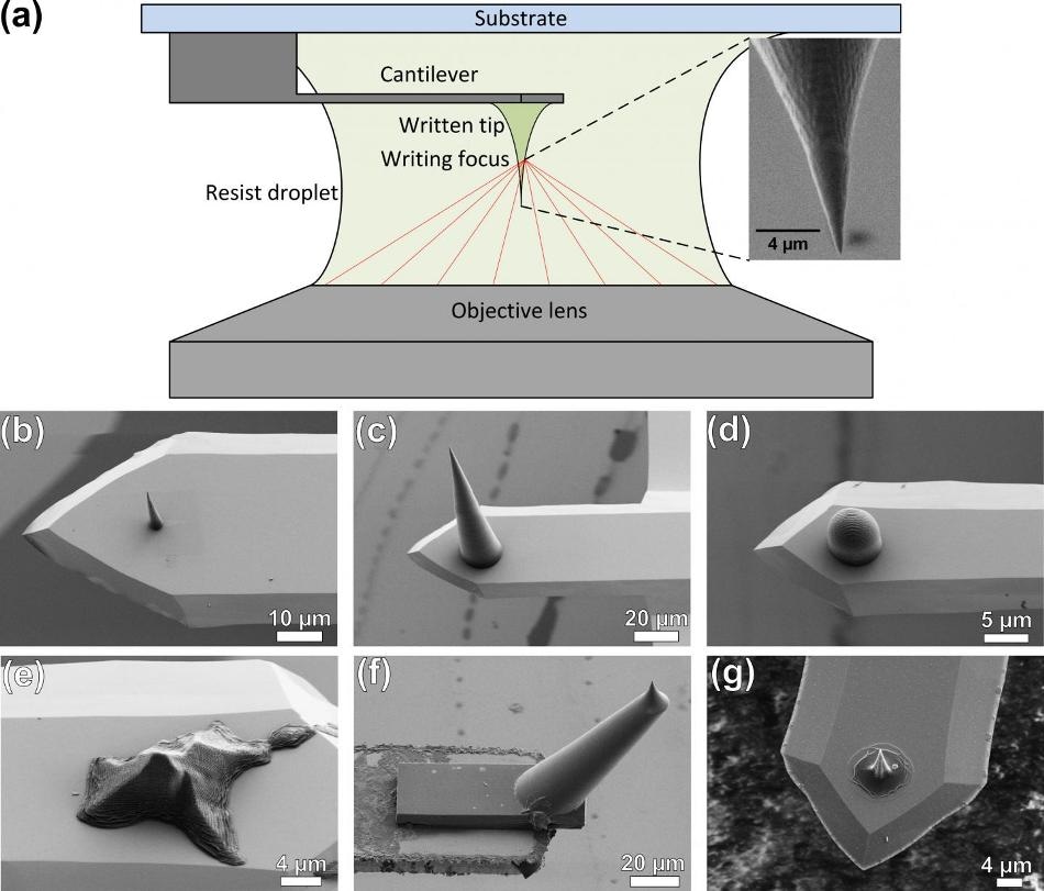
 3D direct laser writing based on two-photon polymerization can be used to create custom-designed tips. (a) Schematic drawing of the writing process on the cantilever using two-photon polymerization. The inset shows a scanning electron microscope image of the tip apex.
Atomic force microscopy (AFM) enables scientists to study surfaces at the atomic level. The technique is based on a basic concept: a pointed tip on a cantilever 'senses' the samples’ topography.
While AFM has been effectively used for over three decades and users can easily access traditional micromachined probes for their experiments, the use of standard-sized tips does not always serve the exact purpose.
Generally, scientists require uniquely designed tips – either extremely long tips or a particular shape of tip apex that can easily reach the base of deep trenches. While micromachining can be used to prepare nonstandard tip, it is reclusively expensive.
Now, a research team at Karlsruhe Institute of Technology (KIT) in Germany has developed a new technique to fabricate customized AFM tips or probes using 3D direct laser writing based on two-photon polymerization. The results of the study will be published on the cover of AIP Publishing’s Applied Physics Letters.
Two-photon polymerization is a 3D printing process, which offers structuring with excellent resolution. This process uses a strongly centered infrared femtosecond laser to reveal a UV-light-curable photoresist material. This material promotes two-photon adsorption, thereby initiating a polymerization reaction. In this fashion, freely designed components can be precisely written at the place of their purpose, including tiny objects like AFM probes on cantilevers.
This concept isn't new at the macroscopic scale: you can freely design any shape with your computer and print it in 3-D. But at the nanoscale, this approach is complex. To write our tips, we applied two-photon polymerization with an experimental setup, recently developed at KIT, which is now available from startup company Nanoscribe GmbH.
Hendrik Hölscher, KIT
According to the team, small tips with radii down to 25 nm - approximately 3,000 times smaller than the width of a single strand of human hair - and random shapes can be joined to traditionally shaped micromachined cantilevers.
Despite this, long-term scanning measurements have revealed low wear rates, demonstrating the reliability of such AFM tips. "We were also able to prove that the resonance spectrum of the probe can be tuned for multi-frequency applications by adding reinforcing structures to the cantilever," Hölscher said.
The ability to fabricate optimal AFM probes could provide unlimited options for sample analysis and that too with dramatically improved resolution.
Writing parts via 3-D printing is expected to become a big business at the macroscopic scale. But I was surprised by how nicely it works for nanoscale, too. When our group started with this project, we tried to continuously stretch the technology's limits ... but Ph.D. students Philipp-Immanuel Dietrich and Gerald Göring kept coming back from the lab with new successful results.
Hendrik Hölscher, KIT
Nanotechnology experts would now be able to use two-photon polymerization in future applications. "We expect other groups working within the field of scanning probe methods to be able to take advantage of our approach as soon as possible," Hölscher noted. "It may even become an Internet business that allows you to design and order AFM probes via the web."
Hölscher added that the researchers will continue to improve their method and apply it to other research projects, spanning from optics and photonics to biomimetics.