Aug 3 2016
Data traffic is growing worldwide. Glass-fiber cables transmit information over long distances at the speed of light. Once they have reached their destination, however, these optical signals have to be converted into electrical signals for subsequent processing in the computer. KIT researchers have now developed a novel type of photodetector that needs far less space than conventional ones. The component has a base area of less than one millionth of a square millimeter without the data transmission rate being affected adversely. The corresponding article is published in the Optica journal. (DOI:10.1364/OPTICA.3.000741)
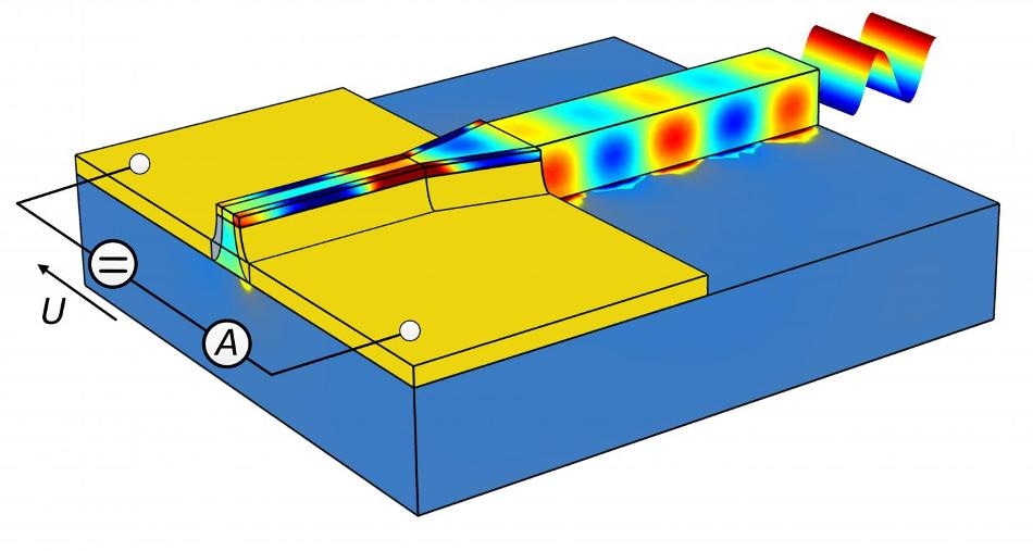
 A plasmonic detector that is directly coupled to a silicon optical waveguide and smaller than one micrometer was developed by KIT.(Credit: Graphics: KIT)
The newly developed photodetectors, the smallest photodetectors worldwide for optical data transmission, can be used for integrated optical circuits that significantly enhance the performance of optical communication systems. Due to the small space needed, many detectors can be assembled on optical chips. In experiments, the researchers reached a data rate of up to 40 gigabits per second. “This component can transmit the contents of a complete DVD within a fraction of a second,” physicist Sascha Mühlbrandt of KIT explains. He conducted his studies at the Institute of Microstructure Technology and the Institute of Photonics and Quantum Electronics of KIT. This rate can be even further increased. “It is the so far smallest detector reaching this data rate. It is one hundred times smaller than a conventional photodetector,” Mühlbrandt emphasizes. The high-speed photodetector, called PIPED (Plasmonic Internal Photoemission Detector), is now presented by Mühlbrandt as first author, together with colleagues of KIT and ETH Zurich, in the Optica journal under the heading “Silicon-Plasmonic Internal-Photoemission Detector for 40 Gbit/s Data Reception.”
A special advantage of the reduced size is that the photodetector can be integrated with electronic components on the same CMOS chip. “Introduction of novel plasmonic components for high-speed transmission of information between electronic chips in the computer combines the advantages of electronic and optical components, while the transmission rate is comparable or even improved,” says project coordinator Professor Manfred Kohl of KIT’s Institute of Microstructure Technology. The photodetector was developed under the NAVOLCHI (Nano Scale Disruptive Silicon-Plasmonic Platform for Chip-to-Chip Interconnection) project. Under the 7th EU Research Framework Programme, the KIT project of three years’ duration in the area of information and communication technologies was funded with about EUR 500,000.
The high-performance photodetector uses so-called surface plasmon polaritons, highly concentrated electromagnetic waves at metallic-dielectric interfaces, to combine optics and electronics on smallest space. “This new class of plasmonic transceivers is based on the mechanism generating photocurrent, i.e. direct signal conversion at metallic interfaces with optical frequencies. This process is known as internal photoemission,” Mühlbrandt says. For enhancing the efficiency of light absorption and light conversion into electrical signals, charge carriers are generated at a titanium-silicon transition and taken up at another gold-silicon transition. The high rate is due to the special detector geometry: Both metal-silicon transitions are located less than one hundred billionth of a meter apart.
The researchers consider the PIPED concept to be essential not only for future optical data transmission systems, but also for wireless data transmission. “This novel approach to detecting optical signals allows for the generation and detection of electromagnetic signals with bandwidths in the terahertz range,” says Professor Christian Koos of KIT, Spokesperson of the Helmholtz International Research School for Teratronics (HIRST) that focuses on the combination of photonic and electronic processes for ultra-rapid signal processing. “Plasmonic components might be used in wireless high-speed communication and allow for transmission rates of up to 1 terabit per second. “Research related to PIPED was also supported by the EnTeraPIC Starting Grant of the European Research Council, the Helmholtz International Research School for Teratronics (HIRST) at KIT, at which the disciplines of physics, electrical engineering, computer science, and mechanical engineering cooperate, as well as by KIT’s “Karlsruhe Nano-Micro Facility” (KNMF) platform.
S. Mühlbrandt, A. Melikyan, T. Harter, K. Köhnle, A. Muslija, P. Vincze, S. Wolf, P. Jakobs, Y. Fedoryshyn, W. Freude, J. Leuthold, C. Koos, M. Kohl: Silicon-Plasmonic Internal-Photoemission Detector for 40 Gbit/s Data Reception. Optica. DOI: 10.1364/OPTICA.3.000741,
https://www.osapublishing.org/optica/abstract.cfm?uri=optica-3-7-741
Information on NAVOLCHI: http://www.imt.kit.edu/projects/navolchi/