Mar 10 2014
Using an inexpensive inkjet printer, University of Utah electrical engineers produced microscopic structures that use light in metals to carry information. This new technique, which controls electrical conductivity within such microstructures, could be used to rapidly fabricate superfast components in electronic devices, make wireless technology faster or print magnetic materials.
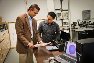
 University of Utah electrical engineers Ajay Nahata and Barun Gupta used a $60 inkjet printer with silver and carbon ink cartridges to create a new, widely applicable way to make microscopic structures that use light in metals to carry information. This new technique could be used to rapidly fabricate superfast components in electronic devices, make wireless technology faster or print magnetic materials. Credit: Dan Hixson, University of Utah College of Engineering.
The study appears online March 7 in the journal Advanced Optical Materials.
High-speed Internet and other data-transfer techniques rely on light transported through optical fibers with very high bandwidth, which is a measure of how fast data can be transferred. Shrinking these fibers allows more data to be packed into less space, but there’s a catch: optical fibers hit a limit on how much data they can carry as light is squeezed into smaller and smaller spaces.
In contrast, electronic circuits can be fashioned at much smaller sizes on silicon wafers. However, electronic data transfer operates at frequencies with much lower bandwidth, reducing the amount of data that can be carried.
A recently discovered technology called plasmonics marries the best aspects of optical and electronic data transfer. By crowding light into metal structures with dimensions far smaller than its wavelength, data can be transmitted at much higher frequencies such as terahertz frequencies, which lie between microwaves and infrared light on the spectrum of electromagnetic radiation that also includes everything from X-rays to visible light to gamma rays. Metals such as silver and gold are particularly promising plasmonic materials because they enhance this crowding effect.
“Very little well-developed technology exists to create terahertz plasmonic devices, which have the potential to make wireless devices such as Bluetooth – which operates at 2.4 gigahertz frequency – 1,000 times faster than they are today,” says Ajay Nahata, a University of Utah professor of electrical and computer engineering and senior author of the new study.
Using a commercially available inkjet printer and two different color cartridges filled with silver and carbon ink, Nahata and his colleagues printed 10 different plasmonic structures with a periodic array of 2,500 holes with different sizes and spacing on a 2.5-inch-by-2.5 inch plastic sheet.
The four arrays tested had holes 450 microns in diameter – about four times the width of a human hair – and spaced one-25th of an inch apart. Depending on the relative amounts of silver and carbon ink used, the researchers could control the plasmonic array’s electrical conductivity, or how efficient it was in carrying an electrical current.
“Using a $60 inkjet printer, we have developed a low-cost, widely applicable way to make plasmonic materials,” Nahata says. “Because we can draw and print these structures exactly as we want them, our technique lets you make rapid changes to the plasmonic properties of the metal, without the million-dollar instrumentation typically used to fabricate these structures.”
Plasmonic arrays are currently made using microfabrication techniques that require expensive equipment and manufacture only one array at a time. Until now, controlling conductivity in these arrays has proven extremely difficult for researchers.
Nahata and his co-workers at the University of Utah’s College of Engineering used terahertz imaging to measure the effect of printed plasmonic arrays on a beam of light. When light with terahertz frequency is directed at a periodic array of holes in a metal layer, it can result in resonance, a fundamental property best illustrated by a champagne flute shattering when it encounters a musical tone of the right pitch.
Terahertz imaging is useful for nondestructive testing, such as detection of anthrax bacterial weapons in packaging or examination of insulation in spacecraft. By studying how terahertz light transmits through their printed array, the Utah team showed that simply changing the amount of carbon and silver ink used to print the array could be used to vary transmission through this structure.
With this new printing technique, Nahata says, “we have an extra level of control over both the transmission of light and electrical conductivity in these devices – you can now design structures with as many different variations as the printer can produce.”
Nahata says these faster plasmonic arrays eventually could prove useful for:
- Wireless devices, because the arrays allow data to be transmitted much more quickly. Many research groups are actively working on this application now.
- Printing magnetic materials for greater functionality (lower conductivity, more compact) in different devices. This technology is more than five years away, Nahata says.
Although the Utah team used two different kinds of ink, up to four different inks in a four-color inkjet printer could be used, depending on the application.
Nahata conducted this study with University of Utah electrical and computer engineering graduate students Barun Gupta and Shashank Pandey, and Sivaraman Guruswamy, professor of metallurgical engineering at the university. The study was funded by the National Science Foundation through the University of Utah’s Materials Research Science and Engineering Center.
University of Utah College of Engineering
72 S. Central Campus Dr., Room 1650 WEB
Salt Lake City, UT 84112
801-581-6911 fax: 801-581-8692
www.coe.utah.edu