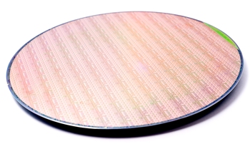
Imec announced today the launch of its fully integrated silicon photonics platform through a cost-sharing Multi-Project Wafer (MPW) service via ePIXfab. The platform enables cost-effective R&D of silicon photonic ICs for high-performance optical transceivers (25Gb/s and beyond) and optical sensing and life science applications.

The offered integrated components include low-loss waveguides, efficient grating couplers, high-speed silicon electro-optic modulators and high-speed germanium waveguide photo-detectors.
Since 2007, imec and its associated laboratory at Ghent University have been offering a platform for passive silicon photonic components via ePIXfab*, for R&D under shared cost conditions. Now, imec extends its silicon photonics offering, using a standard130nm CMOS toolset, with active components such as high-speed optical modulators and integrated germanium photo-detectors.
“Imec’s Silicon Photonics platform provides robust performance and solutions to integrated photonics products in medical diagnostics, telecom and datacom industries. Companies can benefit from our silicon photonics capability through established standard cells, or explore the functionality of their own designs in MPW,” stated Philippe Absil, program director at imec. “This Silicon Photonics MPW offer provides a cost-efficient solution, with state-of-the-art performance, design flexibility and superior CD and thickness control”.
The first run opens for registration with tape-in on 9th of Oct 2013 and first devices will be out in May 2014. Support, registration and design kit access will be organized by Europractice IC service, in collaboration with world-wide MPW partners.
Imec’s Si Photonics 200mm wafer platform offers extensive design flexibility and includes –
- Tight within-wafer silicon thickness variation 3 < 2.5nm
- 3-level patterning of 220nm top Si layer (193nm optical lithography)
- poly-Si overlay and patterning (193nm optical lithography)
- 3-level n-type implants and 3-level p-type implants in Si
- Ge epitaxial growth on Si and p-type and n-type implants in Ge
- Local NiSi contacts, Tungsten vias and Cu metal interconnects
- Al bond pads
- Validated cell library with fiber couplers, polarization rotators, highly efficient carrier depletion modulators and ultra-compact Ge waveguide photo-detectors with low dark current.
- Design kit support for Ipkiss, PhoeniX and Mentor Graphics software