Nov 27 2012
A new device invented at the Harvard School of Engineering and Applied Sciences (SEAS) can absorb 99.75% of infrared light that shines on it. When activated, it appears black to infrared cameras.
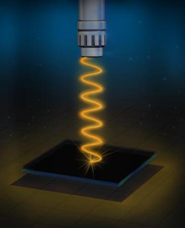
 This is an artist's rendition of the experimental setup used to measure the reflectivity of the vanadium-sapphire device. (Credit: Modified from an illustration by Kirill Nadtochiy.)
Composed of just a 180-nanometer-thick layer of vanadium dioxide (VO2) on top of a sheet of sapphire, the device reacts to temperature changes by reflecting dramatically more or less infrared light.
Announced today in the journal Applied Physics Letters, and featured on its cover, this perfect absorber is ultrathin, tunable, and exceptionally well suited for use in a range of infrared optical devices.
Perfect absorbers have been created many times before, but not with such versatile properties. In a Fabry-Pérot cavity, for instance, two mirrors sandwich an absorbing material, and light simply reflects light back and forth until it's mostly all gone. Other devices incorporate surfaces with nanoscale metallic patterns that trap and eventually absorb the light.
"Our structure uses a highly unusual approach, with better results," says principal investigator Federico Capasso, Robert L. Wallace Professor of Applied Physics and Vinton Hayes Senior Research Fellow in Electrical Engineering at SEAS. "We exploit a kind of naturally disordered metamaterial, along with thin-film interference effects, to achieve one of the highest absorption rates we've ever seen. Yet our perfect absorber is structurally simpler than anything tried before, which is important for many device applications."
With collaborators at Harvard and at the University of California, San Diego, Capasso's research group took advantage of surprising properties in both of the materials they used.
Vanadium dioxide is normally an insulating material, meaning that it does not conduct electricity well. Take it from room temperature up to about 68 degrees Celsius, however, and it undergoes a dramatic transition. The crystal quickly rearranges itself as the temperature approaches a critical value. Metallic islands appear as specks, scattered throughout the material, with more and more appearing until it has become uniformly metallic.
"Right near this insulator-to-metal transition, you have a very interesting mixed medium, made up of both insulating and metallic phases," says coauthor Shriram Ramanathan, Associate Professor of Materials Science at SEAS, who synthesized the thin film. "It's a very complex and rich microstructure in terms of its electronic properties, and it has very unusual optical properties."
Those properties, when manipulated correctly, happen to be ideal for infrared absorption.
Meanwhile, the underlying sapphire substrate has a secret of its own. Usually transparent, its crystal structure actually makes it opaque and reflective, like a metal, to a narrow subset of infrared wavelengths.
The result is a combination of materials that internally reflects and devours incident infrared light.
"Both of these materials have lots of optical losses, and we've demonstrated that when light reflects between lossy materials, instead of transparent or highly reflective ones, you get strange interface reflections," explains lead author Mikhail Kats, a graduate student at SEAS. "When you combine all of those resulting waves, you can coax them to destructively interfere and completely cancel out. The net effect is that a film one hundred times thinner than the wavelength of the incident light can create perfect absorption."
The challenge for Capasso, Ramanathan, Kats, and their colleagues was not only to understand this behavior, but also to learn how to fabricate pure enough samples of the vanadium dioxide.
"Vanadium oxide can exist in many oxidation states, and only if you have VO2 does it go through a metal-insulator transition close to room temperature," Ramanathan explains. "We have developed several techniques in our lab to allow exquisite compositional and structural control, almost at the atomic scale, to grow such complex films. The resulting phase purity allows us to see these remarkable properties, which otherwise would be very difficult to observe."
Because the device can be easily switched between its absorbent and non-absorbent states, the possible applications are quite wide ranging and include bolometers (thermal imaging devices) with tunable absorption, spectroscopy devices, tunable filters, thermal emitters, radiation detectors, and equipment for energy harvesting.
"An ideal bolometer design needs to absorb all of the infrared light that falls on it, turning it to heat, and correspondingly its resistance should change a lot per degree change in temperature," notes Kats. "In principle, our new perfect absorber could be used to make incredibly sensitive thermal cameras."
Harvard's Office of Technology Development has filed patent applications on the novel invention and is actively pursuing licensing and commercialization opportunities.