Fast and ultrasensitive optical systems are gaining increasing significance and are being used in a diverse range of applications, for example, in imaging procedures in the fields of medicine and biology, in astronomy and in safety engineering for the automotive industry.
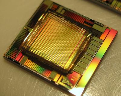
 It is now possible to process digital image signals directly on the microchip. Credit: Fraunhofer IMS
Frequently the challenge lies in being able to record high-quality images under extremely low light conditions. Modern photo detectors for image capture typically reach their limits here. They frequently work with light-sensitive electronic components that are based on CMOS (Complementary Metal Oxide Semiconductor) or CCD (Charge-Coupled Device) image sensors. The problem is that neither the latest CMOS nor CCD systems can simultaneously guarantee a swift and highly-sensitive high quality image recording if there is a paucity of photons to read.
In cooperation with the partners of the MiSPiA project consortium the Fraunhofer Institute for Microelectronic Circuits and Systems IMS in Duisburg has now advanced the development of CMOS technology and introduced an ultrasensitive image sensor with this technology, based on Single Photon Avalanche Photodiodes (SPAD). Its pixel structure can count individual photons within a few picoseconds, and is therefore a thousand times faster than comparable models. Since each individual photon is taken into consideration camera images are also possible with extremely weak light sources.
Camera installed directly on chip
To achieve this the new image sensor uses the "internal avalanche breakdown effect"– a photoelectric amplification effect. The number of "avalanche breakdowns" corresponds to the number of photons that the pixels hit. In order to count these events, each of the sensor's pixels comes with very precise digital counters. At the same time, the scientists have applied microlenses to each sensor chip, which focus the incoming beam in each pixel onto the photoactive surface. Another advantage is that processing the digital image signals is already possible directly on the microchip; therefore, additional analogue signal processing is no longer needed.
"The image sensor is a major step toward digital image generation and image processing. It allows us to have the capability to use even very weak light sources for photography. The new technology installs the camera directly on the semiconductor, and is capable of turning the information from the light into images at a significantly faster pace," states Dr. Daniel Durini, group manager for optical components at the Fraunhofer Institute IMS.
IMS engineered the sensor under the European research project MiSPiA (Microelectronic Single-Photon 3D Imaging Arrays for low-light high-speed Safety and Security Applications). Altogether, seven partners throughout Europe from the fields of research and business are involved in the project. In the next stage, the scientists from Duisburg are working on a process to produce sensors that are back-lighted, and in this regard, even more powerful. At the same time, the new technology is already being utilized in tests for traffic. Chip-based mini-cameras protect vehicles, bicycles and pedestrians from collisions and chip-based accidents, or assist in the reliable functioning of safety belts and airbags.